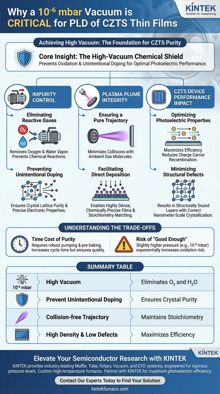
Achieving a background pressure of 10⁻⁶ mbar is critical for removing atmospheric contaminants that compromise the chemical integrity of CZTS thin films. This specific vacuum level is required to evacuate impurity gases—primarily oxygen and water vapor—preventing them from reacting with the material during the sensitive deposition phase.
The Core Insight A high-vacuum environment acts as a chemical shield, ensuring the laser-generated plasma plume travels through a pristine path to the substrate. By preventing oxidation and unintentional doping, this pressure level guarantees the structural purity required for optimal photoelectric performance in CZTS semiconductors.
The Imperative of Impurity Control
Eliminating Reactive Gases
The primary function of reaching 10⁻⁶ mbar is the removal of residual atmosphere. Without this deep vacuum, gases such as oxygen and water vapor remain in the chamber.
These gases are chemically reactive and will readily bond with the CZTS material. Even trace amounts of moisture can degrade the quality of the final film.
Preventing Unintentional Doping
Semiconductors like CZTS are highly sensitive to their atomic composition. The presence of background gases can lead to unintentional doping, where foreign atoms embed themselves into the crystal lattice.
This alters the electronic properties of the film in uncontrolled ways. Maintaining 10⁻⁶ mbar ensures that only the intended target material forms the semiconductor layer.
Preserving Plasma Plume Integrity
Ensuring a Pure Trajectory
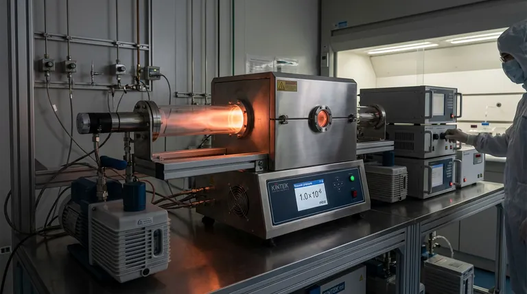
During Pulsed Laser Deposition (PLD), a laser ablates the target material to create a high-energy plasma plume.
This plume must travel from the target to the substrate without interference. A high-vacuum environment allows this plume to propagate through a "clean" space, minimizing collisions with ambient gas molecules.
Facilitating Direct Deposition
By minimizing interference, the sputtered atomic flux deposits directly onto the substrate.
This unobstructed path allows for the growth of highly dense and chemically precise films. It ensures the stoichiometry (chemical balance) of the deposited film matches the target material as closely as possible.
Impact on CZTS Device Performance
Optimizing Photoelectric Properties
For CZTS films, the ultimate goal is energy conversion. Impurities act as defects that trap charge carriers, reducing the efficiency of the material.
The high purity afforded by the 10⁻⁶ mbar vacuum is essential for maximizing photoelectric performance. It ensures the electrons can move freely, which is vital for the semiconductor's function.
Minimizing Structural Defects
A clean vacuum environment leads to defect-free growth.
When foreign particles are excluded, the film can crystallize correctly on the nanometer scale. This results in a structurally sound layer that is less prone to degradation over time.
Understanding the Trade-offs
The Time Cost of Purity
Achieving 10⁻⁶ mbar requires time and robust pumping systems. It often necessitates pre-baking the chamber to drive off water vapor and carbon oxides desorbing from the internal walls.
This increases the cycle time for each batch of films. However, rushing this process invariably leads to inferior material quality.
The Risk of "Good Enough"
It may be tempting to operate at slightly higher pressures (e.g., 10⁻⁵ mbar) to save time.
However, in semiconductor fabrication, this is a critical error. The exponential increase in gas molecules at lower vacuum levels dramatically raises the probability of oxidation, rendering the CZTS film unsuitable for high-performance applications.
Making the Right Choice for Your Goal
To ensure your CZTS thin films meet performance standards, evaluate your process against these criteria:
- If your primary focus is Maximum Photoelectric Efficiency: Strictly adhere to the 10⁻⁶ mbar threshold (or lower) to eliminate all potential recombination centers caused by oxygen or water impurities.
- If your primary focus is Process Consistency: Implement a rigorous pre-baking protocol for your vacuum chamber to ensure you hit the base pressure of 10⁻⁶ mbar reliably before every deposition run.
Ultimately, the vacuum level is not just a setting; it is a fundamental manufacturing variable that dictates the purity and viability of your semiconductor device.
Summary Table:
| Feature | Requirement in PLD | Impact on CZTS Thin Films |
|---|---|---|
| Vacuum Level | 10⁻⁶ mbar (High Vacuum) | Eliminates atmospheric contaminants like O₂ and H₂O |
| Impurity Control | Prevent Unintentional Doping | Ensures precise electronic properties and crystal lattice purity |
| Plume Dynamics | Collision-free Trajectory | Maintains stoichiometric transfer from target to substrate |
| Film Quality | High Density & Low Defects | Maximizes photoelectric efficiency and charge carrier mobility |
Elevate Your Semiconductor Research with KINTEK
Precise CZTS thin film deposition starts with a superior vacuum environment. KINTEK provides industry-leading Muffle, Tube, Rotary, Vacuum, and CVD systems, specifically engineered to achieve the rigorous pressure levels required for high-performance lab applications.
Backed by expert R&D and manufacturing, our high-temperature furnaces are fully customizable to meet your unique research needs. Don't compromise on film purity—partner with KINTEK to ensure your materials achieve maximum photoelectric efficiency.
Contact Our Experts Today to Find Your Solution
Visual Guide
References
- Serap Yi̇ği̇t Gezgi̇n, Hamdi Şükür Kılıç. Microstrain effects of laser-ablated Au nanoparticles in enhancing CZTS-based 1 Sun photodetector devices. DOI: 10.1039/d4cp00238e
This article is also based on technical information from Kintek Furnace Knowledge Base .
Related Products
- RF PECVD System Radio Frequency Plasma Enhanced Chemical Vapor Deposition
- Custom Made Versatile CVD Tube Furnace Chemical Vapor Deposition CVD Equipment Machine
- Inclined Rotary Plasma Enhanced Chemical Deposition PECVD Tube Furnace Machine
- Multi Heating Zones CVD Tube Furnace Machine for Chemical Vapor Deposition Equipment
- Slide PECVD Tube Furnace with Liquid Gasifier PECVD Machine
People Also Ask
- What are the system specifications of the PECVD system? Unlock Precision Thin-Film Deposition
- What is the role of RF power in PECVD and how does the RF-PECVD process work? Master Thin Film Deposition Control
- What are some promising applications of PECVD-prepared 2D materials? Unlock Advanced Sensing and Optoelectronics
- What are the applications of plasma enhanced chemical vapor deposition? Key Uses in Electronics, Optics & Materials
- What is RF in PECVD? A Critical Control for Plasma Deposition


