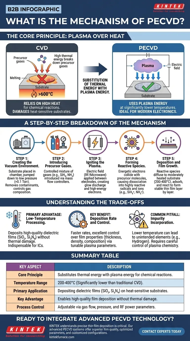
At its core, Plasma-Enhanced Chemical Vapor Deposition (PECVD) is a process that uses plasma to deposit thin films onto a substrate. Unlike conventional Chemical Vapor Deposition (CVD), which relies on high temperatures to drive chemical reactions, PECVD uses the energy of an ionized gas to achieve deposition at significantly lower temperatures. This makes it an essential technique for manufacturing modern electronics and other heat-sensitive devices.
The fundamental mechanism of PECVD is the substitution of thermal energy with plasma energy. By applying an electric field to precursor gases in a vacuum, the process creates a low-temperature plasma filled with reactive species that readily deposit onto a substrate, forming a high-quality thin film without requiring damaging high heat.
The Core Principle: Plasma Over Heat
To understand PECVD, you must first understand the problem it solves. Traditional CVD requires very high temperatures (often >600°C) to provide enough energy to break down precursor gases and initiate film-forming reactions.
The Limitation of High Temperature
Many advanced materials, particularly in semiconductor manufacturing, cannot withstand extreme heat. A fully processed silicon wafer with intricate, multi-layered circuits would be damaged or destroyed by the high temperatures of traditional CVD.
This creates a critical need for a deposition method that works at lower temperatures while still producing high-quality films.
How Plasma Provides the Energy
PECVD solves this problem by using plasma, an ionized gas often called the fourth state of matter.
An electric field, typically radio frequency (RF) or microwave, is applied to a low-pressure gas inside the chamber. This field energizes free electrons, which then collide with the neutral precursor gas molecules.
These high-energy collisions transfer energy to the gas molecules, breaking them apart (dissociation) and knocking off other electrons (ionization). This creates a reactive soup of ions, radicals, and other excited species, all at a relatively low overall gas temperature.
A Step-by-Step Breakdown of the Mechanism
The PECVD process can be broken down into five distinct steps that occur inside a specialized vacuum chamber.
Step 1: Creating the Vacuum Environment
First, the substrate (such as a silicon wafer) is placed on an electrode inside a sealed chamber. The chamber is then pumped down to a very low pressure, typically below 0.1 Torr. This vacuum environment serves two purposes: it removes contaminants and allows for precise control of the gas composition.
Step 2: Introducing Precursor Gases
A precisely controlled mixture of precursor gases is introduced into the chamber using mass flow controllers. For example, to deposit silicon nitride (Si₃N₄), gases like silane (SiH₄) and ammonia (NH₃) are used. These are often mixed with inert carrier gases like argon or nitrogen.
Step 3: Igniting the Plasma
An electric field is applied between two electrodes inside the chamber. This powerful field energizes the gas mixture, initiating a glow discharge and creating the plasma. This plasma contains the highly energetic electrons needed for the next step.
Step 4: Forming Reactive Species
The energetic electrons in the plasma collide with the stable precursor gas molecules. These collisions have enough energy to break the chemical bonds of the precursors, dissociating them into highly reactive radicals and ions (e.g., SiH₃•, NH₂•). This is the key "plasma enhancement" step that bypasses the need for high thermal energy.
Step 5: Deposition and Film Growth
These newly formed reactive species diffuse through the chamber and adsorb onto the surface of the substrate, which is often moderately heated (e.g., 200-400°C) to promote surface reactions and improve film quality. On the surface, they react with each other to form a stable, solid thin film, which grows layer by layer.
Understanding the Trade-offs
While PECVD is a powerful technique, it's essential to understand its advantages and the parameters that require careful control.
The Primary Advantage: Low-Temperature Processing
The ability to deposit high-quality dielectric films, such as silicon dioxide (SiO₂) and silicon nitride (Si₃N₄), at low temperatures is the defining advantage of PECVD. This makes it indispensable for creating the insulating and passivating layers in integrated circuits and other complex devices.
Key Benefit: Deposition Rate and Control
PECVD generally offers a faster deposition rate than many other low-temperature techniques. Furthermore, by adjusting parameters like gas flow, pressure, and RF power, operators can fine-tune the plasma density and energy. This provides excellent control over the final film's properties, including its thickness, density, and chemical composition.
Common Pitfall: Impurity Incorporation
Because the reactions happen at lower temperatures, PECVD films can sometimes incorporate unintended elements, most commonly hydrogen from the precursor gases. Controlling the plasma chemistry and deposition parameters is critical to minimize these impurities and ensure the film meets the required electrical and mechanical specifications.
Applying This to Your Goal
Your choice of deposition method depends entirely on the requirements of your substrate and the desired film properties.
- If your primary focus is depositing films on heat-sensitive substrates: PECVD is the clear choice, as its use of plasma energy is specifically designed to avoid thermal damage.
- If your primary focus is process speed and tunable film properties: PECVD offers a fast, controllable process for a wide range of materials, making it a versatile tool for both research and production.
- If your primary focus is achieving the highest possible film purity and density: You must carefully optimize your PECVD recipe, as some high-temperature CVD processes may inherently produce films with fewer impurities for certain materials.
By leveraging plasma to enable chemistry at low temperatures, PECVD stands as a cornerstone technology that makes modern microfabrication possible.
Summary Table:
| Key Aspect | Description |
|---|---|
| Core Principle | Substitutes thermal energy with plasma energy for chemical reactions |
| Temperature Range | 200-400°C (significantly lower than traditional CVD) |
| Primary Application | Depositing dielectric films (SiO₂, Si₃N₄) on heat-sensitive substrates |
| Key Advantage | Enables high-quality film deposition without thermal damage |
| Process Control | Adjustable via gas flow, pressure, and RF power parameters |
Ready to integrate advanced PECVD technology into your laboratory?
At KINTEK, we understand that precise thin-film deposition is critical for your research and manufacturing success. Our expertise in high-temperature furnace solutions extends to advanced deposition systems like PECVD, where our strong R&D and deep customization capabilities ensure you get exactly the system you need.
Whether you're working with semiconductor wafers, MEMS devices, or other heat-sensitive materials, we can help you:
- Achieve superior film quality at lower temperatures
- Optimize deposition parameters for your specific application
- Customize system configurations to meet unique experimental requirements
Let's discuss how our PECVD solutions can enhance your thin-film processes. Contact our experts today for a personalized consultation!
Visual Guide
Related Products
- Slide PECVD Tube Furnace with Liquid Gasifier PECVD Machine
- RF PECVD System Radio Frequency Plasma Enhanced Chemical Vapor Deposition
- Inclined Rotary Plasma Enhanced Chemical Deposition PECVD Tube Furnace Machine
- Inclined Rotary Plasma Enhanced Chemical Deposition PECVD Tube Furnace Machine
- Multi Heating Zones CVD Tube Furnace Machine for Chemical Vapor Deposition Equipment
People Also Ask
- What role does a Tube Furnace play in the CVD growth of carbon nanotubes? Achieve High-Purity CNT Synthesis
- What plasma source is used in PE-CVD tube furnaces? Unlock Low-Temperature, High-Quality Deposition
- How does a hydrogen reduction environment in an industrial tube furnace facilitate gold-copper alloy microspheres?
- What are the typical conditions for plasma-enhanced CVD processes? Achieve Low-Temperature Thin Film Deposition
- How does PECVD equipment contribute to TOPCon bottom cells? Mastering Hydrogenation for Maximum Solar Efficiency


