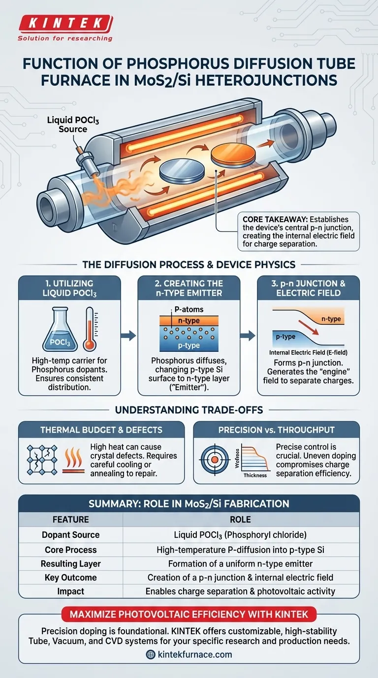
The specific role of a phosphorus diffusion tube furnace in fabricating MoS2/Si heterojunctions is to chemically alter the p-type silicon substrate to create an active electrical component. By utilizing a liquid POCl3 source at high temperatures, the furnace drives phosphorus atoms into the silicon to form an n-type emitter layer.
Core Takeaway: This furnace is responsible for establishing the device's central p-n junction. Without this specific doping step, the silicon substrate would lack the internal electric field necessary to separate charges, rendering the solar cell unable to generate power.
The Diffusion Process Mechanism
Utilizing Liquid POCl3 Sources
The furnace operates by introducing a liquid source, specifically POCl3 (Phosphoryl chloride), into the process chamber.
Under high-temperature conditions, this liquid acts as the carrier for phosphorus dopants. The stability of the tube furnace ensures that the dopant distribution remains consistent across the substrate.
Creating the n-type Emitter
The primary objective is to transform the surface of the p-type silicon substrate.
As phosphorus diffuses into the silicon lattice, it changes the electrical conductivity type of the material. This creates a distinct n-type layer on top of the p-type base, a process known as "emitter formation."
Role in Device Physics
Establishing the p-n Junction
The interaction between the newly formed n-type layer and the original p-type substrate creates a p-n junction.
In the context of MoS2/Si heterojunctions, this silicon-based junction is often the primary driver of photovoltaic activity. It serves as the foundational structure upon which the MoS2 layer operates or interacts.
Generating the Internal Electric Field
The physical creation of the p-n junction naturally results in an internal electric field.
This field is the "engine" of the solar cell. When light strikes the device and creates electron-hole pairs, this field forces the charges to separate, preventing them from recombining and allowing them to be collected as electrical current.
Understanding the Trade-offs
Thermal Budget and Crystal Defects
While diffusion is necessary for doping, the high temperatures required can introduce stress to the silicon wafer.
As noted in broader semiconductor applications, high-heat processes must be carefully managed. Excessive heat or uncontrolled cooling can lead to crystal defects, which may require subsequent annealing steps to repair.
Precision vs. Throughput
Tube furnaces offer excellent stability for batch processing, but they require precise control over gas flow and temperature profiles.
Variations in the diffusion process can lead to uneven doping profiles. If the n-type layer is too thick or too thin, the efficiency of charge separation drops, compromising the overall performance of the MoS2/Si device.
Making the Right Choice for Your Project
The effectiveness of your MoS2/Si heterojunction depends heavily on the quality of the silicon substrate preparation.
- If your primary focus is Electrical Efficiency: Prioritize precise temperature control during the POCl3 diffusion to ensure a uniform n-type emitter depth, which maximizes charge collection.
- If your primary focus is Device Longevity: Ensure the furnace process includes or follows an annealing protocol to heal any crystal lattice damage caused during the high-temperature diffusion.
The phosphorus diffusion step is not merely a surface treatment; it is the fundamental process that activates the silicon substrate for energy conversion.
Summary Table:
| Feature | Role in MoS2/Si Fabrication |
|---|---|
| Dopant Source | Liquid POCl3 (Phosphoryl chloride) |
| Core Process | High-temperature phosphorus diffusion into p-type silicon |
| Resulting Layer | Formation of a uniform n-type emitter |
| Key Outcome | Creation of a p-n junction and internal electric field |
| Impact | Enables charge separation and photovoltaic activity |
Maximize Your Photovoltaic Efficiency with KINTEK
Precision doping is the foundation of high-performance MoS2/Si heterojunctions. At KINTEK, we understand that uniform phosphorus diffusion requires uncompromising temperature stability and gas flow control.
Backed by expert R&D and manufacturing, we offer industry-leading Tube, Vacuum, and CVD systems—along with specialized Rotary and Muffle furnaces—all fully customizable to your specific research or production requirements. Whether you are optimizing electrical efficiency or ensuring device longevity through annealing, our high-temp lab solutions provide the reliability you need.
Ready to elevate your semiconductor fabrication? Contact our experts today to find the perfect furnace for your unique material needs.
Visual Guide
References
- Sel Gi Ryu, Keunjoo Kim. Photoenhanced Galvanic Effect on Carrier Collection of the MOS<sub>2</sub> Contact Layer in Silicon Solar Cells. DOI: 10.1002/pssa.202500039
This article is also based on technical information from Kintek Furnace Knowledge Base .
Related Products
- Slide PECVD Tube Furnace with Liquid Gasifier PECVD Machine
- Custom Made Versatile CVD Tube Furnace Chemical Vapor Deposition CVD Equipment Machine
- Magnesium Extraction and Purification Condensing Tube Furnace
- Multi Heating Zones CVD Tube Furnace Machine for Chemical Vapor Deposition Equipment
- Split Chamber CVD Tube Furnace with Vacuum Station CVD Machine
People Also Ask
- What is plasma in the context of PECVD? Unlock Low-Temperature Thin Film Deposition
- What are the disadvantages of tube furnace cracking when processing heavy raw materials? Avoid Costly Downtime and Inefficiency
- What role does a Tube Furnace play in the CVD growth of carbon nanotubes? Achieve High-Purity CNT Synthesis
- What are the typical conditions for plasma-enhanced CVD processes? Achieve Low-Temperature Thin Film Deposition
- What are the main advantages of PECVD tube furnaces compared to CVD tube furnaces? Lower Temp, Faster Deposition, and More