In materials science and manufacturing, Physical Vapor Deposition (PVD) is a family of vacuum-based processes used to create high-performance thin films and coatings. The core principle involves physically transforming a solid material into a vapor, transporting it through a vacuum, and allowing it to condense onto a substrate's surface. This method is distinct from chemical processes as it relies on physical mechanics, such as bombardment or evaporation.
PVD is not a single technique, but a versatile toolbox for enhancing a material's surface properties. By physically, rather than chemically, transferring atoms in a vacuum, it allows engineers to apply extremely thin, high-purity coatings to improve hardness, wear resistance, or appearance.
How PVD Works: The Core Principle
PVD is fundamentally a line-of-sight transfer process that occurs in a vacuum chamber. The entire process can be broken down into three essential stages.
The Vacuum Environment
All PVD processes take place under a high vacuum. This is critical to prevent the vaporized coating material from reacting with or being scattered by atoms in the air, ensuring a pure, dense film.
The Three-Step Process
First, energy is introduced to a solid source material, called a target, causing it to transform into a vapor. This is the generation stage.
Second, this vapor travels through the vacuum chamber from the source to the object being coated, known as the substrate. This is the transport stage.
Finally, the vapor condenses on the substrate, forming a thin, tightly bonded film. This is the deposition stage.
Key PVD Methods Explained
While many PVD variations exist, two of the most common methods are Sputtering and Thermal Evaporation. They differ primarily in how they generate the material vapor.
Sputtering: A "Billiard Ball" Collision
In sputtering, the substrate is placed in a vacuum chamber with the target. High-energy ions (typically of an inert gas like Argon) are accelerated to strike the target.
This impact is like a microscopic game of billiards, where the ions act as cue balls, knocking atoms loose from the target material. These ejected atoms then travel and deposit onto the substrate.
Thermal Evaporation: A "Boiling" Process
Thermal evaporation is conceptually simpler. The source material is heated in the vacuum chamber until it reaches a temperature where it begins to evaporate or sublime, transitioning directly into a gaseous phase.
This vapor then rises, travels through the chamber, and condenses as a solid film on the cooler surface of the substrate.
Understanding the Advantages and Trade-offs
PVD is a powerful technology, but it is essential to understand its capabilities and limitations compared to other processes, such as Chemical Vapor Deposition (CVD).
Advantage: Material Versatility
Because it is a physical process, PVD can be used to deposit a vast range of inorganic materials, including metals, alloys, and ceramics. This makes it extremely flexible for different applications.
Advantage: High Deposition Rates
PVD processes are generally faster than CVD. This makes PVD a strong candidate for applications requiring high throughput or the rapid deposition of thicker films.
Trade-off: Line-of-Sight Deposition
A key limitation of most PVD processes is that the coating material travels in a straight line. If a part of the substrate is in a "shadow" and not directly visible to the source, it will not get coated evenly, making it challenging for complex 3D shapes.
Trade-off: Lower "Throwing Power"
Related to the line-of-sight issue, PVD has difficulty coating the inside of deep holes or complex internal geometries. Processes like CVD, which use a reactive gas that can flow into these areas, often perform better in this regard.
Making the Right Choice for Your Goal
Selecting the right coating technology depends entirely on your specific objective and the geometry of your part.
- If your primary focus is creating durable, wear-resistant surfaces on tools or components: PVD is an industry standard for applying hard coatings like Titanium Nitride (TiN) and Diamond-Like Carbon (DLC).
- If your primary focus is high-throughput manufacturing or applying decorative films: PVD's speed and ability to produce brilliant, metallic finishes make it a superior choice for many consumer products.
- If your primary focus is coating complex, non-line-of-sight geometries: You may need to explore specialized PVD fixture setups or consider an alternative process like Chemical Vapor Deposition (CVD) to ensure uniform coverage.
By understanding its physical principles and practical trade-offs, you can leverage PVD to precisely engineer the surface of almost any material.
Summary Table:
| Aspect | Details |
|---|---|
| Process Type | Physical vapor deposition in vacuum |
| Key Methods | Sputtering, Thermal Evaporation |
| Main Advantages | High deposition rates, material versatility |
| Key Limitations | Line-of-sight deposition, lower throwing power |
| Common Applications | Wear-resistant coatings, decorative films |
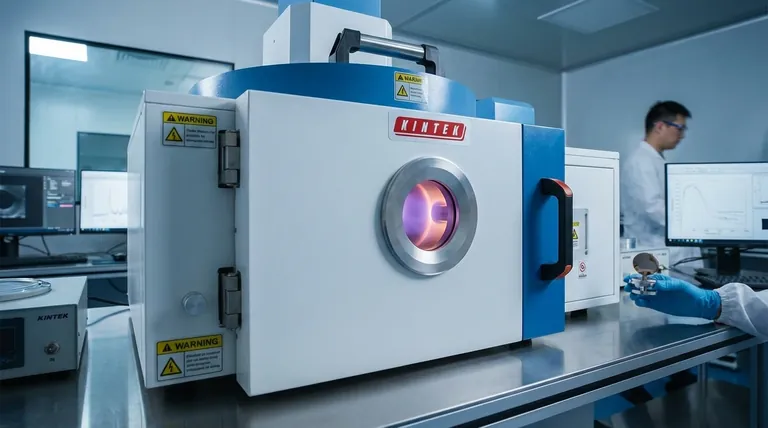
Elevate your lab's capabilities with KINTEK's advanced PVD solutions! Leveraging exceptional R&D and in-house manufacturing, we provide diverse laboratories with high-temperature furnace systems like CVD/PECVD, tailored to your unique needs. Our deep customization ensures precise thin film coatings for enhanced material performance. Contact us today to discuss how we can optimize your processes and drive innovation!
Visual Guide
