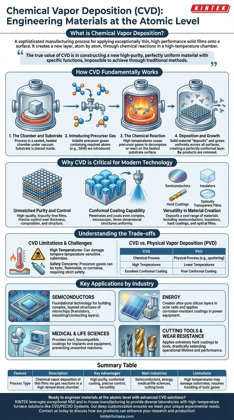
At its core, Chemical Vapor Deposition (CVD) is a sophisticated manufacturing process used to apply an exceptionally thin, high-performance solid film onto a surface. It achieves this by introducing a precursor gas into a high-temperature chamber, which then chemically reacts and bonds to a substrate, effectively building a new layer atom by atom. This technique is indispensable in industries like semiconductors, energy, and life sciences, where material properties at the microscopic level are critical.
The true value of CVD is not merely in coating a surface, but in constructing a new one. It enables the creation of high-purity, perfectly uniform materials with specific functions that are impossible to achieve through traditional methods.
How CVD Fundamentally Works
To understand why CVD is so crucial, you must first grasp the elegance of its process. It is a thermochemical method that transforms a gas into a solid, high-performance film.
The Chamber and Substrate
The entire process takes place inside a sealed reaction chamber, often under a vacuum. The object to be coated, known as the substrate, is placed inside this chamber.
Introducing the Precursor Gas
One or more volatile gases, called precursors, are introduced into the chamber. These precursors contain the specific atoms required for the final coating (e.g., silicon from silane gas).
The Chemical Reaction
The chamber is heated to extremely high temperatures. This thermal energy causes the precursor gases to decompose or react with each other on the surface of the heated substrate.
Deposition and Growth
As the chemical reaction occurs, the desired solid material "deposits" onto the substrate. This film grows uniformly across all exposed surfaces, creating a perfectly conformal layer that follows every microscopic contour of the object. Unwanted chemical by-products are continuously removed from the chamber.
Why CVD is Critical for Modern Technology
The precise nature of the CVD process gives it unique advantages that are essential for manufacturing advanced components across multiple industries.
Unmatched Purity and Control
Because the process is built from a controlled chemical reaction with pure gases, the resulting films are incredibly high-quality and free of impurities. Engineers can precisely control the film's thickness, composition, and crystalline structure by managing temperature, pressure, and gas flow.
Conformal Coating Capability
Unlike a spray-on coating, the gas precursors in CVD can penetrate and coat even the most complex, microscopic, three-dimensional structures. This ability to create a uniform layer everywhere is a defining feature and is non-negotiable for applications like integrated circuits.
Versatility in Material Creation
CVD is not limited to one type of material. The process can be adapted to deposit a vast range of materials, including:
- Semiconductors (e.g., silicon)
- Insulators (e.g., silicon dioxide)
- Hard, protective coatings (e.g., titanium nitride)
- Optically transparent films
Understanding the Trade-offs
While powerful, CVD is not a universal solution. Its requirements introduce specific limitations and challenges that must be considered.
The Challenge of High Temperatures
The high heat required for most CVD processes can damage or warp temperature-sensitive substrates, such as many plastics or certain metal alloys. This limits the types of materials that can be coated effectively.
Precursor and Safety Concerns
The precursor gases used in CVD can be highly toxic, flammable, or corrosive. Handling and disposing of these materials requires stringent safety protocols and specialized, expensive equipment.
CVD vs. Physical Vapor Deposition (PVD)
CVD is often compared to Physical Vapor Deposition (PVD), another thin-film technique. While PVD processes (like sputtering) are physical rather than chemical and can operate at lower temperatures, they typically struggle to produce the highly conformal coatings that are CVD's primary strength.
Key Applications by Industry
Your choice to use CVD depends entirely on the material properties you need to achieve.
- If your primary focus is Semiconductors: CVD is the foundational technology used to build the complex, layered structures of microchips, depositing the insulating and conducting layers that form transistors.
- If your primary focus is Energy: CVD is used to create the ultra-pure silicon layers in solar cells and to apply corrosion-resistant coatings inside power generation equipment.
- If your primary focus is Medical & Life Sciences: CVD provides inert, biocompatible coatings for medical implants and analytical equipment, preventing unwanted reactions with the human body or sensitive samples.
- If your primary focus is Cutting Tools & Wear Resistance: CVD applies extremely hard coatings to industrial drill bits and cutting tools, drastically extending their operational lifetime and performance.
Ultimately, CVD empowers us to engineer materials at the atomic level, building the foundation for the next generation of technology.
Summary Table:
| Feature | Description |
|---|---|
| Process Type | Chemical vapor deposition of thin films via gas reactions in a high-temperature chamber |
| Key Advantages | High purity, conformal coating, precise control, versatility in materials (e.g., semiconductors, insulators) |
| Main Industries | Semiconductors, energy, medical/life sciences, cutting tools |
| Limitations | High temperatures may damage substrates; requires handling of toxic gases |
Ready to engineer materials at the atomic level with advanced CVD solutions? KINTEK leverages exceptional R&D and in-house manufacturing to provide diverse laboratories with high-temperature furnace solutions like CVD/PECVD Systems. Our strong deep customization capability ensures we precisely meet your unique experimental needs. Contact us today to discuss how our products can enhance your research and production in semiconductors, energy, and beyond!
Visual Guide
Related Products
- Custom Made Versatile CVD Tube Furnace Chemical Vapor Deposition CVD Equipment Machine
- Multi Heating Zones CVD Tube Furnace Machine for Chemical Vapor Deposition Equipment
- HFCVD Machine System Equipment for Drawing Die Nano Diamond Coating
- Split Chamber CVD Tube Furnace with Vacuum Station CVD Machine
- 915MHz MPCVD Diamond Machine Microwave Plasma Chemical Vapor Deposition System Reactor
People Also Ask
- What customization options are available for CVD tube furnaces? Tailor Your System for Superior Material Synthesis
- How does CVD tube furnace sintering enhance graphene growth? Achieve Superior Crystallinity and High Electron Mobility
- What is a CVD tube furnace and what is its primary function? Discover Precision Thin-Film Deposition
- What is the working principle of a CVD tube furnace? Achieve Precise Thin Film Deposition for Your Lab
- What are the practical applications of gate media prepared by CVD tube furnaces? Unlock Advanced Electronics and More


