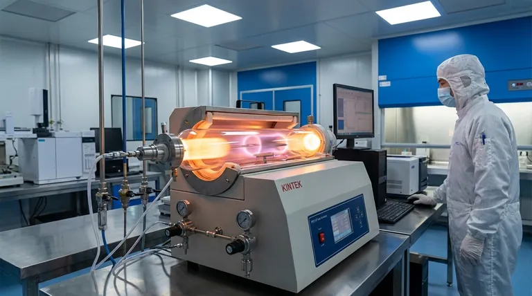
At its core, Chemical Vapor Deposition (CVD) is a method for building high-performance solid materials atom by atom. It is a manufacturing process that uses controlled chemical reactions in a gaseous state to deposit an exceptionally pure and durable thin film onto a substrate. This technique is fundamental to creating advanced components for industries ranging from semiconductors and optics to aerospace and energy.
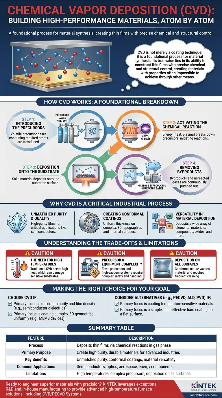
Chemical Vapor Deposition is not merely a coating technique; it is a foundational process for material synthesis. Its true value lies in its ability to construct thin films with precise chemical and structural control, creating materials with properties often impossible to achieve through other means.
How CVD Works: A Foundational Breakdown
To understand CVD, it is best to view it as a precise, multi-stage chemical recipe performed within a sealed reaction chamber. Each stage is critical to the final quality of the deposited film.
Step 1: Introducing the Precursors
The process begins by introducing one or more volatile precursor gases into a reaction chamber. These precursors are chemical compounds that contain the atoms required for the final film. For example, to create a silicon film, a precursor like silane gas (SiH₄) might be used.
Step 2: Activating the Chemical Reaction
Energy is applied to the system to break down the precursor gases and initiate the chemical reactions. Most commonly, this energy is heat, with the substrate being heated to several hundred or even over a thousand degrees Celsius. This is known as thermal CVD. Other variants use plasma (Plasma-Enhanced CVD, or PECVD) or light (Photo-assisted CVD) to drive the reaction, often at lower temperatures.
Step 3: Deposition onto the Substrate
As the precursor gases decompose and react near the hot substrate, they form a solid material that deposits onto the surface. This deposition occurs across all exposed surfaces, building a thin, solid film. The process is controlled to ensure the film has the desired thickness, density, and chemical composition.
Step 4: Removing Byproducts
The chemical reactions produce the desired solid film as well as gaseous byproducts. These byproducts, along with any unreacted precursor gases, are continuously pumped out of the reaction chamber, ensuring a clean process and a pure final material.
Why CVD is a Critical Industrial Process
CVD is not used because it is simple or cheap; it is used because the quality of the material it produces is often unparalleled. The benefits directly address the needs of high-technology manufacturing.
Unmatched Purity and Quality
Because the process starts with highly purified gases and involves specific chemical reactions, the resulting films are exceptionally pure and dense. This is critical for applications like semiconductors, where even minuscule impurities can ruin a microchip's performance.
Creating Conformal Coatings
A key advantage of CVD is its ability to create conformal coatings. This means the film deposits with a uniform thickness over complex, three-dimensional topographies, covering steps, trenches, and internal surfaces perfectly. This is something that line-of-sight deposition methods (like PVD) cannot easily achieve.
Versatility in Material Deposition
The CVD process is remarkably versatile and can be adapted to deposit a wide array of materials. This includes elemental materials (like silicon), compounds (like silicon nitride or titanium carbide), metal oxides, sulfides, and more. This flexibility allows engineers to create custom material layers for specific functions.
Understanding the Trade-offs and Limitations
No process is perfect. An objective evaluation of CVD requires acknowledging its inherent challenges, which often define whether it is the right choice for an application.
The Need for High Temperatures
Traditional thermal CVD processes require very high temperatures. This heat can damage or alter the properties of the underlying substrate, especially if it contains plastics, pre-existing electronic circuits, or other temperature-sensitive materials.
Precursor and Equipment Complexity
The precursor gases used in CVD can be highly toxic, flammable, or corrosive, requiring sophisticated safety protocols and handling equipment. The high-vacuum and high-temperature systems themselves are complex and expensive to purchase and maintain.
Deposition on All Surfaces
The same conformal nature that makes CVD powerful can also be a drawback. The process deposits the film on every exposed surface inside the chamber, including the chamber walls and tooling, not just the intended substrate. This can lead to wasted material and require frequent cleaning cycles.
Making the Right Choice for Your Goal
Selecting a deposition method depends entirely on the technical requirements and economic constraints of your project. CVD is a high-performance tool for demanding applications.
- If your primary focus is maximum purity and film density: CVD is often the superior choice for applications like semiconductor gate dielectrics, where material quality is non-negotiable.
- If your primary focus is coating complex 3D geometries uniformly: The conformal nature of CVD makes it ideal for coating intricate parts, such as MEMS devices or the internal surfaces of components.
- If your primary focus is coating temperature-sensitive materials: You must look at lower-temperature CVD variants like Plasma-Enhanced CVD (PECVD) or Atomic Layer Deposition (ALD), as traditional thermal CVD is likely unsuitable.
- If your primary focus is a simple, cost-effective hard coating on a flat surface: Other methods, like Physical Vapor Deposition (PVD), might offer a more economical solution if the absolute conformality of CVD is not required.
Ultimately, understanding CVD allows you to select a process that builds your material from the atoms up, ensuring its properties are engineered for performance.
Summary Table:
| Feature | Description |
|---|---|
| Process | Deposits thin films via chemical reactions in gas phase |
| Primary Purpose | Create high-purity, durable materials for advanced industries |
| Key Benefits | Unmatched purity, conformal coatings, material versatility |
| Common Applications | Semiconductors, optics, aerospace, energy components |
| Limitations | High temperatures, complex precursors, deposition on all surfaces |
Ready to engineer superior materials with precision? KINTEK leverages exceptional R&D and in-house manufacturing to provide advanced high-temperature furnace solutions, including CVD/PECVD Systems, tailored for diverse laboratories. Our strong deep customization capability ensures we meet your unique experimental needs—contact us today to discuss how we can enhance your research and production!
Visual Guide
Related Products
- 915MHz MPCVD Diamond Machine Microwave Plasma Chemical Vapor Deposition System Reactor
- Custom Made Versatile CVD Tube Furnace Chemical Vapor Deposition CVD Equipment Machine
- RF PECVD System Radio Frequency Plasma Enhanced Chemical Vapor Deposition
- MPCVD Machine System Reactor Bell-jar Resonator for Lab and Diamond Growth
- HFCVD Machine System Equipment for Drawing Die Nano Diamond Coating
People Also Ask
- What factors influence the quality of diamond deposition in the MPCVD method? Master the Critical Parameters for High-Quality Diamond Growth
- What are some key features and benefits of the microwave plasma chemical vapor deposition system? Achieve Unmatched Material Synthesis
- What are the essential components of an MPCVD reactor for diamond film deposition? Unlock High-Quality Diamond Growth
- What are the main components of an MPCVD machine? Unlock the Secrets of Diamond Synthesis
- What are the essential components of an MPCVD reactor system? Build a Pristine Environment for High-Purity Materials


