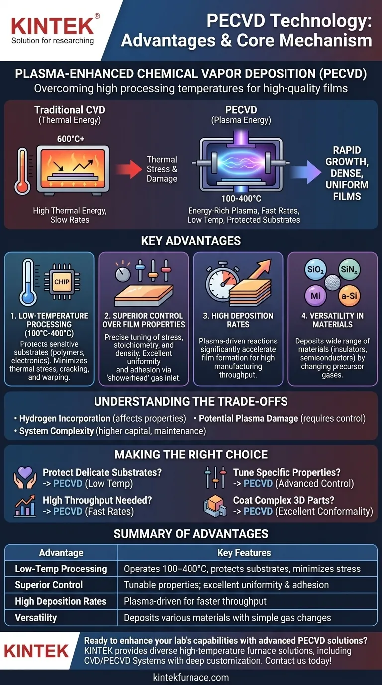
At its core, Plasma-Enhanced Chemical Vapor Deposition (PECVD) overcomes a primary limitation of traditional deposition techniques: high processing temperatures. Its main advantages are the ability to deposit high-quality films at low temperatures, excellent control over film properties, high deposition rates, and the versatility to create a wide range of materials, from insulators to semiconductors.
PECVD breaks the dependency on high thermal energy to drive chemical reactions. Instead, it uses an energy-rich plasma, allowing for the rapid growth of dense, uniform thin films at temperatures low enough to protect even the most delicate underlying substrates.

The Core Mechanism: How Plasma Changes the Game
To understand the advantages of PECVD, you must first understand its fundamental difference from conventional Chemical Vapor Deposition (CVD).
Overcoming the Thermal Budget
Traditional CVD requires very high temperatures, often over 600°C, to provide the thermal energy needed to break down precursor gases and initiate chemical reactions on a substrate surface.
PECVD replaces most of this thermal energy with energy from a plasma. By applying a strong radio frequency (RF) electric field to a low-pressure gas, we create a highly reactive environment of ions and radicals, all at a much lower overall temperature.
Accelerating Deposition Rates
Because the plasma creates a high concentration of reactive species, the surface chemical reactions that form the film happen much more quickly than in thermally-driven processes. This results in significantly higher deposition rates, which is a critical factor for manufacturing throughput.
Key Advantage 1: Low-Temperature Processing
The most significant advantage of PECVD is its ability to operate at low temperatures, typically in the range of 100°C to 400°C.
Protecting Sensitive Substrates
This low-temperature window makes it possible to deposit films on materials that would be damaged or destroyed by conventional CVD temperatures. This includes polymers, plastics, and fully-fabricated semiconductor devices with low melting point metals.
Minimizing Thermal Stress
High temperatures cause materials to expand and contract. This introduces significant mechanical stress in the deposited film, which can lead to cracking, delamination, or warping of the substrate. PECVD’s lower temperatures dramatically reduce this thermal stress.
Key Advantage 2: Superior Control Over Film Properties
The use of plasma provides additional control levers that are not available in traditional CVD, allowing for precise tuning of the final film.
Achieving Excellent Uniformity and Adhesion
PECVD systems often use a "showerhead" gas inlet. This distributes the precursor gases evenly over the substrate, resulting in films with excellent thickness uniformity. The energetic plasma also promotes strong adhesion between the film and the substrate.
Tuning Stress, Stoichiometry, and Density
By adjusting process parameters like pressure, gas flow, and plasma power, engineers can precisely control the film's final properties. For example, mixing high and low RF frequencies is a common technique to tune the film's intrinsic mechanical stress from compressive to tensile. This allows for the creation of highly-engineered layers for specific optical or electronic performance.
Depositing a Vast Range of Materials
PECVD is exceptionally versatile. The same system can be used to deposit a wide array of materials simply by changing the precursor gases. This includes dielectric insulators like silicon dioxide (SiO₂) and silicon nitride (SiNₓ), amorphous silicon for solar cells, and even conductive layers.
Understanding the Trade-offs
No technology is without its considerations. An objective analysis requires understanding PECVD's potential challenges.
The Role of Hydrogen
PECVD precursor gases are often hydrogen-based (e.g., silane, SiH₄). As a result, deposited films frequently incorporate hydrogen, which can affect the film's electrical and optical properties. While this can be managed, it is a key difference from higher-temperature, hydrogen-free films.
Potential for Plasma-Induced Damage
The same energetic ions that enable low-temperature deposition can, if not properly controlled, cause damage to the substrate surface or the growing film. Modern PECVD process control is designed to carefully manage this ion bombardment.
System Complexity
A PECVD system, with its RF power supplies, vacuum chambers, and matching networks, is more complex and capital-intensive than a simple thermal CVD furnace. This complexity requires more sophisticated process control and maintenance.
Making the Right Choice for Your Application
Selecting the right deposition method depends entirely on your project's primary goal.
- If your primary focus is protecting delicate electronics or polymer substrates: PECVD is the definitive choice, as its low processing temperature prevents thermal damage.
- If your primary focus is high manufacturing throughput for dielectric layers: PECVD's plasma-driven high deposition rates offer a significant advantage over many conventional CVD and PVD methods.
- If your primary focus is tuning a specific film property like mechanical stress: The advanced process controls of PECVD, such as dual-frequency tuning, offer unparalleled fine-tuning.
- If your primary focus is coating complex 3D parts uniformly: PECVD provides excellent conformality, creating an even coating that is superior to line-of-sight techniques like sputtering.
Ultimately, PECVD provides a powerful synthesis of deposition speed, film quality, and process safety that unlocks new capabilities in materials science and advanced manufacturing.
Summary Table:
| Advantage | Key Features |
|---|---|
| Low-Temperature Processing | Operates at 100°C-400°C, protects sensitive substrates, minimizes thermal stress |
| Superior Control Over Film Properties | Tunable stress, stoichiometry, density; excellent uniformity and adhesion |
| High Deposition Rates | Plasma-driven reactions for faster throughput |
| Versatility | Deposits insulators, semiconductors, and more with simple gas changes |
| Trade-offs | Hydrogen incorporation, potential plasma damage, system complexity |
Ready to enhance your lab's capabilities with advanced PECVD solutions? Leveraging exceptional R&D and in-house manufacturing, KINTEK provides diverse laboratories with high-temperature furnace solutions, including CVD/PECVD Systems. Our strong deep customization capability precisely meets your unique experimental needs for low-temperature, high-quality film deposition. Contact us today to discuss how we can support your projects!
Visual Guide
Related Products
- Slide PECVD Tube Furnace with Liquid Gasifier PECVD Machine
- RF PECVD System Radio Frequency Plasma Enhanced Chemical Vapor Deposition
- Inclined Rotary Plasma Enhanced Chemical Deposition PECVD Tube Furnace Machine
- Inclined Rotary Plasma Enhanced Chemical Deposition PECVD Tube Furnace Machine
- Multi Heating Zones CVD Tube Furnace Machine for Chemical Vapor Deposition Equipment
People Also Ask
- What are the disadvantages of tube furnace cracking when processing heavy raw materials? Avoid Costly Downtime and Inefficiency
- How does a hydrogen reduction environment in an industrial tube furnace facilitate gold-copper alloy microspheres?
- What are the typical conditions for plasma-enhanced CVD processes? Achieve Low-Temperature Thin Film Deposition
- What are the advantages of using a tube furnace CVD system for Cu(111)/graphene? Superior Scalability and Quality
- What plasma source is used in PE-CVD tube furnaces? Unlock Low-Temperature, High-Quality Deposition


