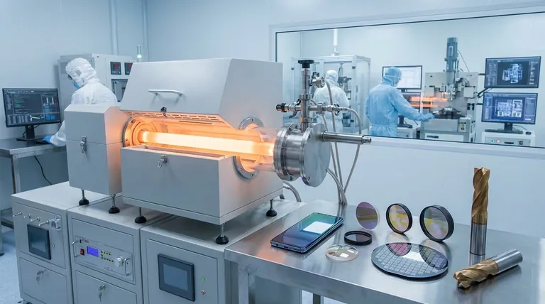
From your smartphone to industrial tools, the influence of Plasma-Enhanced Chemical Vapor Deposition (PECVD) is widespread. PECVD is a critical manufacturing process used to deposit high-quality thin films for semiconductor devices, advanced optics, and protective industrial coatings. Its primary commercial advantage is the ability to perform this deposition at low temperatures, enabling the use of substrates that would be damaged by the intense heat of traditional methods.
The commercial power of PECVD lies in its ability to bypass the high-temperature limitations of conventional deposition techniques. By using an energized plasma instead of extreme heat, it enables the creation of uniform, high-purity thin films on materials that are sensitive to thermal damage, unlocking a vast range of modern technological applications.
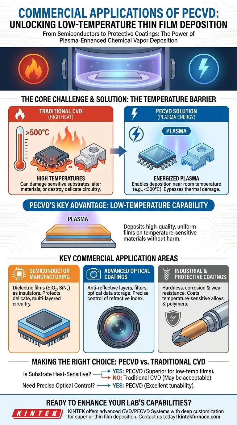
The Core Problem PECVD Solves: The Temperature Barrier
To understand PECVD's applications, you must first understand the fundamental problem it solves. The goal of any chemical vapor deposition process is to create a solid thin film on a surface from gaseous precursors.
The Limitation of Traditional CVD
Conventional Chemical Vapor Deposition (CVD) relies on very high temperatures to provide the energy needed to break down precursor gases and drive the chemical reactions that form the film.
This high heat, often several hundred degrees Celsius, is a significant constraint.
Why High Temperature Is a Problem
Many modern materials and complex devices simply cannot withstand such temperatures. For example, high heat can melt plastic substrates, alter the properties of certain metals, or destroy the delicate, multi-layered circuitry already fabricated on a semiconductor wafer.
The PECVD Solution: Plasma as the Energy Source
PECVD masterfully circumvents this issue. Instead of relying solely on thermal energy, it uses an electromagnetic field (typically radio frequency) to ignite the precursor gases into a state of matter called plasma.
This plasma is a highly energetic environment that provides the activation energy for the chemical reactions. This allows for the deposition of dense, high-quality films at much lower temperatures, often near room temperature.
Key Commercial Application Areas
This low-temperature capability is the gateway to PECVD's most important commercial uses.
Semiconductor Manufacturing
PECVD is indispensable in the fabrication of microelectronics. It is used to deposit dielectric films, such as silicon dioxide (SiO₂) and silicon nitride (SiNₓ), which act as insulators between conductive layers.
Because modern chips contain billions of transistors built in complex vertical stacks, depositing a new layer cannot damage the intricate circuitry that already exists underneath. PECVD is the go-to method for this critical task.
Advanced Optical Coatings
The technology is instrumental in producing a wide array of optical coatings. This includes anti-reflective layers on sunglasses and camera lenses, filters used in scientific instruments like photometers, and layers for optical data storage.
The key advantage here is precise control. By carefully managing the plasma parameters—such as gas composition, pressure, and power—engineers can meticulously tune the refractive index and other optical properties of the deposited film.
Industrial and Protective Coatings
PECVD is used to apply thin films that enhance the properties of industrial tools and components. These coatings can provide hardness, corrosion resistance, and wear resistance.
Because the process is low-temperature, these protective benefits can be applied to a wider range of materials, including temperature-sensitive alloys and even some polymers, that could not be coated using traditional high-temperature CVD.
Understanding the Trade-offs and Advantages
While powerful, PECVD is a specific tool chosen for its distinct benefits over other methods.
The Primary Advantage: Low Temperature
This cannot be overstated. The ability to deposit films on temperature-sensitive substrates is the single most important commercial driver for PECVD.
Film Quality and Uniformity
The controlled plasma environment allows for the growth of films that are highly uniform across large surfaces and have high density. This leads to higher quality layers with reduced internal stress and less susceptibility to cracking.
Potential Pitfalls to Manage
The use of an energetic plasma is not without its challenges. The process requires careful control to prevent unwanted side effects, such as plasma-induced damage to the substrate surface from ion bombardment. Engineers must fine-tune their process to balance deposition rate with film quality.
Making the Right Deposition Choice
The decision to use PECVD hinges entirely on the thermal budget of your substrate and the required performance of the film.
- If your primary focus is depositing on heat-sensitive substrates: PECVD is often the default and superior solution for achieving high-quality films without damaging the underlying material.
- If your primary focus is creating precise optical layers: PECVD offers the exceptional control over the refractive index and film thickness necessary for anti-reflective or filtering applications.
- If your primary focus is maximum film purity on a robust substrate: Traditional high-temperature CVD may still be preferred in specific cases where the substrate's heat tolerance is not a concern and trace impurities from the plasma are unacceptable.
Ultimately, PECVD's value is its ability to engineer advanced materials under conditions that were previously impossible, making it a foundational process in modern technology.
Summary Table:
| Application Area | Key Uses | Primary Benefit |
|---|---|---|
| Semiconductor Manufacturing | Dielectric films (e.g., SiO₂, SiNₓ) for insulation | Low-temperature deposition prevents damage to delicate circuitry |
| Advanced Optical Coatings | Anti-reflective layers, filters, optical data storage | Precise control of refractive index and film properties |
| Industrial and Protective Coatings | Hardness, corrosion, and wear resistance on tools | Applies to temperature-sensitive materials like alloys and polymers |
Ready to enhance your lab's capabilities with advanced high-temperature furnace solutions? KINTEK leverages exceptional R&D and in-house manufacturing to provide diverse laboratories with cutting-edge equipment, including Muffle, Tube, Rotary Furnaces, Vacuum & Atmosphere Furnaces, and CVD/PECVD Systems. Our strong deep customization capability ensures we can precisely meet your unique experimental requirements, helping you achieve superior results in thin film deposition and material processing. Contact us today to discuss how we can support your projects!
Visual Guide
Related Products
- Slide PECVD Tube Furnace with Liquid Gasifier PECVD Machine
- RF PECVD System Radio Frequency Plasma Enhanced Chemical Vapor Deposition
- Inclined Rotary Plasma Enhanced Chemical Deposition PECVD Tube Furnace Machine
- Inclined Rotary Plasma Enhanced Chemical Deposition PECVD Tube Furnace Machine
- Multi Heating Zones CVD Tube Furnace Machine for Chemical Vapor Deposition Equipment
People Also Ask
- In which industries is the tube furnace commonly used? Essential for Materials Science, Energy, and More
- What are the disadvantages of tube furnace cracking when processing heavy raw materials? Avoid Costly Downtime and Inefficiency
- How does PECVD equipment contribute to TOPCon bottom cells? Mastering Hydrogenation for Maximum Solar Efficiency
- What are the typical conditions for plasma-enhanced CVD processes? Achieve Low-Temperature Thin Film Deposition
- What role does a Tube Furnace play in the CVD growth of carbon nanotubes? Achieve High-Purity CNT Synthesis


