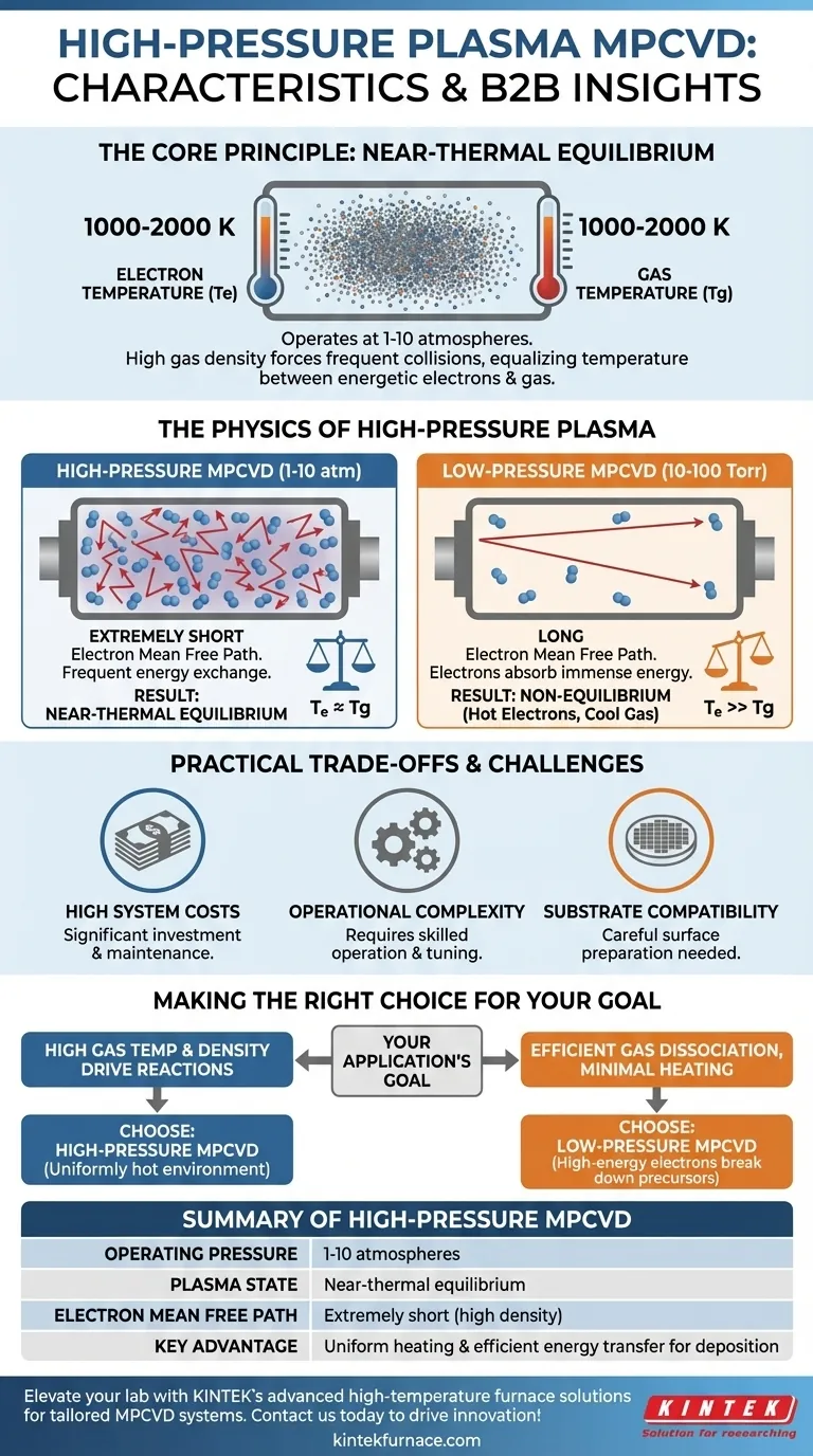
In essence, high-pressure plasma MPCVD operates at gas pressures between 1 and 10 atmospheres. This high-pressure environment forces the plasma into a state of near-thermal equilibrium, where both electrons and neutral gas particles share a similar, moderately high temperature of 1000-2000 K. This state is a direct consequence of a shortened mean free path for the electrons within the dense gas.
The defining characteristic of high-pressure MPCVD is its operation in a near-thermal equilibrium state. Unlike low-pressure methods, the high gas density forces frequent collisions, effectively equalizing the temperature between the energetic electrons and the surrounding gas.
The Physics of High-Pressure Plasma
To understand the unique behavior of high-pressure MPCVD, we must first examine how pressure dictates the plasma's fundamental properties.
The Role of Gas Pressure (1-10 atm)
The process is defined by its operating pressure, which is substantially higher than traditional vacuum-based plasma systems. This high-pressure regime means the reaction chamber is densely packed with gas molecules.
The Impact on Electron Mean Free Path
Mean free path refers to the average distance a particle, like an electron, travels before colliding with another particle.
In the dense environment of high-pressure MPCVD, the mean free path for electrons is extremely short. They cannot travel far before hitting a neutral gas molecule.
Achieving Near-Thermal Equilibrium
Because electrons collide so frequently with gas particles, they efficiently transfer their energy absorbed from the microwaves. This constant energy exchange prevents electrons from becoming significantly hotter than the gas they are in.
The result is a plasma in near-thermal equilibrium, where the electron temperature (Te) is approximately equal to the gas temperature (Tg).
Resulting Temperature Profile (1000-2000 K)
Both electrons and neutral gaseous species stabilize in a temperature range of 1000-2000 K. This is hot enough to drive the desired chemical reactions for material deposition but avoids the extreme temperature differences seen in other plasma types.
High-Pressure vs. Low-Pressure MPCVD: A Critical Comparison
The characteristics of high-pressure MPCVD become clearest when contrasted directly with its low-pressure counterpart.
The Low-Pressure Environment (10-100 Torr)
Low-pressure systems operate at a fraction of atmospheric pressure. This creates a far less dense environment with a long electron mean free path.
The Temperature Imbalance (Non-Equilibrium)
In a low-pressure plasma, electrons travel long distances between collisions, allowing them to absorb immense energy from the microwave field.
This creates a state of non-equilibrium, where electrons become extremely hot (several thousand Kelvin) while the bulk gas remains relatively cool (often below 1000 K).
Implications of the Difference
The choice between high and low pressure fundamentally alters the energy distribution within the plasma. High-pressure uses thermal energy of the bulk gas, while low-pressure relies on the kinetic energy of hyper-energetic electrons to drive reactions.
Understanding the Practical Trade-offs
While powerful, the MPCVD technique carries inherent challenges that apply across different pressure regimes.
High System Costs
The initial purchase and ongoing maintenance of MPCVD systems represent a significant financial investment.
Operational Complexity
Operating an MPCVD system effectively requires deep technical expertise. The process is not "plug-and-play" and demands a skilled operator for tuning and troubleshooting.
Substrate Compatibility
Success often hinges on the substrate material. Careful and often complex surface preparation may be required to ensure proper material growth and adhesion.
Making the Right Choice for Your Goal
Your application's specific requirements will determine whether a high-pressure or low-pressure regime is more suitable.
- If your primary focus is on reactions driven by high gas temperature and density: High-pressure MPCVD is the logical choice, as its near-thermal equilibrium provides a uniformly hot environment.
- If your primary focus is efficient gas dissociation with minimal heating of the substrate: Low-pressure MPCVD is often superior, as its high-energy electrons effectively break down precursor gases without dramatically heating the bulk gas.
Ultimately, understanding the relationship between pressure and plasma equilibrium is the key to selecting and optimizing the correct MPCVD process for your specific material goals.
Summary Table:
| Characteristic | Description |
|---|---|
| Operating Pressure | 1-10 atmospheres |
| Plasma State | Near-thermal equilibrium |
| Electron Mean Free Path | Extremely short due to high gas density |
| Temperature Range | 1000-2000 K for electrons and gas |
| Key Advantage | Uniform heating and efficient energy transfer for material deposition |
Elevate your laboratory's capabilities with KINTEK's advanced high-temperature furnace solutions! Leveraging exceptional R&D and in-house manufacturing, we provide diverse labs with tailored MPCVD systems, including Muffle, Tube, Rotary Furnaces, Vacuum & Atmosphere Furnaces, and CVD/PECVD Systems. Our strong deep customization capability ensures precise alignment with your unique experimental needs, such as optimizing high-pressure plasma processes for superior material growth. Don't settle for less—contact us today to discuss how we can enhance your research and drive innovation!
Visual Guide
Related Products
- 915MHz MPCVD Diamond Machine Microwave Plasma Chemical Vapor Deposition System Reactor
- MPCVD Machine System Reactor Bell-jar Resonator for Lab and Diamond Growth
- Cylindrical Resonator MPCVD Machine System for Lab Diamond Growth
- RF PECVD System Radio Frequency Plasma Enhanced Chemical Vapor Deposition
- Slide PECVD Tube Furnace with Liquid Gasifier PECVD Machine
People Also Ask
- What is the MPCVD method and why is it considered effective for diamond deposition? Superior Purity & High Growth Rates
- What is the purpose of a microwave plasma chemical vapor deposition system? Grow High-Purity Diamonds and Advanced Materials
- What factors influence the quality of diamond deposition in the MPCVD method? Master the Critical Parameters for High-Quality Diamond Growth
- How does the MPCVD process work to deposit diamond? A Guide to High-Purity Synthesis
- What are the essential components of an MPCVD reactor for diamond film deposition? Unlock High-Quality Diamond Growth


