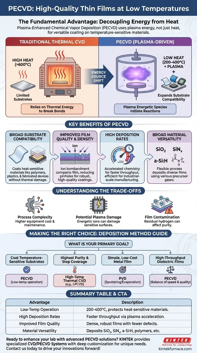
The fundamental advantage of PECVD is its ability to deposit high-quality thin films at significantly lower temperatures than traditional Chemical Vapor Deposition (CVD) methods. By using an energy-rich plasma to drive chemical reactions instead of high heat, PECVD unlocks the ability to coat temperature-sensitive materials like plastics, polymers, and complex electronic devices without causing thermal damage.
PECVD's core value lies in decoupling the energy required for deposition from thermal heat. This single principle makes it uniquely versatile, enabling a combination of low-temperature processing, high deposition rates, and the creation of dense, high-quality films on a vast range of substrates.
The Core Mechanism: Plasma-Driven Chemistry
To understand PECVD's advantages, you must first understand how it differs from traditional thermal processes.
Traditional CVD Relies on Heat
In a standard thermal CVD process, precursor gases must be heated to very high temperatures (often >600°C). This thermal energy is necessary to break chemical bonds and initiate the reactions that lead to film deposition.
This high-heat requirement severely limits the types of materials that can be used as substrates.
PECVD Replaces Heat with Plasma
PECVD operates at much lower temperatures (typically 200-400°C) because it introduces a new energy source: plasma.
An electrical field is used to ionize the precursor gases, creating a plasma—a highly reactive environment of ions, electrons, and free radicals. These energetic species can initiate chemical reactions and deposit a film without the need for intense thermal energy.
Key Benefits of PECVD
This plasma-driven, low-temperature mechanism creates several distinct advantages over other methods like thermal CVD and Physical Vapor Deposition (PVD).
Expands Substrate Compatibility
This is the most significant advantage. PECVD allows for deposition on materials that would melt, deform, or be damaged by high-temperature processes.
This includes polymers, plastics, and fully-fabricated semiconductor wafers with pre-existing metallic structures.
Improves Film Quality and Density
The ion bombardment that occurs during the PECVD process can have a beneficial effect. It compacts the growing film, resulting in a denser, more robust coating with fewer pinholes compared to some other low-temperature methods.
This leads to high-quality films with excellent electrical and mechanical properties, crucial for applications in semiconductors and optics.
Enables High Deposition Rates
The highly reactive plasma environment accelerates the deposition chemistry. Consequently, PECVD can achieve significantly higher deposition rates than PVD techniques like sputtering, especially for dielectric materials.
This makes it highly efficient for industrial-scale manufacturing where throughput is a critical factor.
Offers Broad Material Versatility
The plasma process is flexible and can be used with a wide range of precursor gases. This allows for the deposition of a diverse array of materials.
Common examples include silicon dioxide (SiO₂), silicon nitride (SiNₓ), amorphous silicon (a-Si:H), and even some polymers, providing immense flexibility for device fabrication.
Understanding the Trade-offs
No technology is without its limitations. True expertise requires understanding not just the benefits but also the potential downsides.
Process and Equipment Complexity
PECVD systems are more complex than jejich thermal CVD or PVD counterparts. They require radio-frequency (RF) power supplies, impedance matching networks, and sophisticated process controls to maintain a stable plasma.
This added complexity can translate to higher initial equipment costs and maintenance overhead.
Potential for Plasma-Induced Damage
The same energetic ions that improve film density can also cause damage to the substrate or the growing film if the process is not carefully controlled. This is a particular concern in the fabrication of sensitive electronic devices.
Film Contamination
Because PECVD precursors often contain hydrogen (e.g., silane, SiH₄), the resulting films can incorporate a significant amount of residual hydrogen. While sometimes beneficial, this can be detrimental for certain high-performance electronic applications where film purity is paramount.
Making the Right Choice for Your Goal
Selecting a deposition method depends entirely on your project's specific constraints and desired outcomes.
- If your primary focus is coating temperature-sensitive substrates: PECVD is almost always the superior choice due to its low-temperature operation.
- If your primary focus is achieving the highest possible film purity and step coverage: High-temperature thermal CVD (like LPCVD) may be a better option, provided your substrate can withstand the heat.
- If your primary focus is depositing a simple, pure metal film at a low cost: A PVD method like sputtering or evaporation is often more straightforward and economical.
- If your primary focus is high-throughput deposition of dielectric films: PECVD offers an excellent balance acessórios of speed, quality, and low-temperature compatibility.
Ultimately, PECVD is a powerful and versatile tool that solves the critical challenge of depositing high-quality films without high heat.
Summary Table:
| Advantage | Description |
|---|---|
| Low-Temperature Operation | Enables deposition on heat-sensitive materials like plastics and polymers without thermal damage, typically at 200-400°C. |
| High Deposition Rates | Plasma-driven reactions accelerate film growth, offering faster throughput than many PVD methods. |
| Improved Film Quality | Ion bombardment results in dense, robust films with fewer defects, ideal for electronics and optics. |
| Broad Substrate Compatibility | Works with a wide range of materials, including polymers and pre-fabricated semiconductor wafers. |
| Material Versatility | Deposits various films such as silicon dioxide, silicon nitride, and amorphous silicon using flexible precursors. |
Ready to enhance your lab's capabilities with advanced PECVD solutions? Leveraging exceptional R&D and in-house manufacturing, KINTEK provides diverse laboratories with high-temperature furnace systems, including our specialized CVD/PECVD Systems. Our strong deep customization capability ensures precise solutions for your unique experimental needs, from semiconductor fabrication to materials research. Contact us today to discuss how our PECVD technology can drive your innovations forward!
Visual Guide
Related Products
- RF PECVD System Radio Frequency Plasma Enhanced Chemical Vapor Deposition
- Slide PECVD Tube Furnace with Liquid Gasifier PECVD Machine
- Inclined Rotary Plasma Enhanced Chemical Deposition PECVD Tube Furnace Machine
- Inclined Rotary Plasma Enhanced Chemical Deposition PECVD Tube Furnace Machine
- MPCVD Machine System Reactor Bell-jar Resonator for Lab and Diamond Growth
People Also Ask
- How is silicon dioxide deposited from tetraethylorthosilicate (TEOS) in PECVD? Achieve Low-Temperature, High-Quality SiO2 Films
- How does film quality compare between PECVD and CVD? Choose the Best Method for Your Substrate
- What is PECVD specification? A Guide to Choosing the Right System for Your Lab
- What are the key advantages of PECVD technology? Achieve Low-Temperature, High-Quality Thin Film Deposition
- What is RF in PECVD? A Critical Control for Plasma Deposition


