In short, Silicon Nitride (SiN) deposited via PECVD is a highly versatile thin film used for a range of critical applications, most notably as a protective passivation layer in semiconductor manufacturing, a biocompatible coating for medical devices, and as a functional layer in optical components. Its value comes from a unique combination of dielectric, barrier, and mechanical properties that can be achieved at relatively low temperatures.
The central reason for PECVD Silicon Nitride's widespread use is its ability to deposit a dense, stable, and protective film without the high heat that would damage sensitive electronic or polymer-based components. It offers a "best of both worlds" solution: robust protection with a gentle manufacturing process.
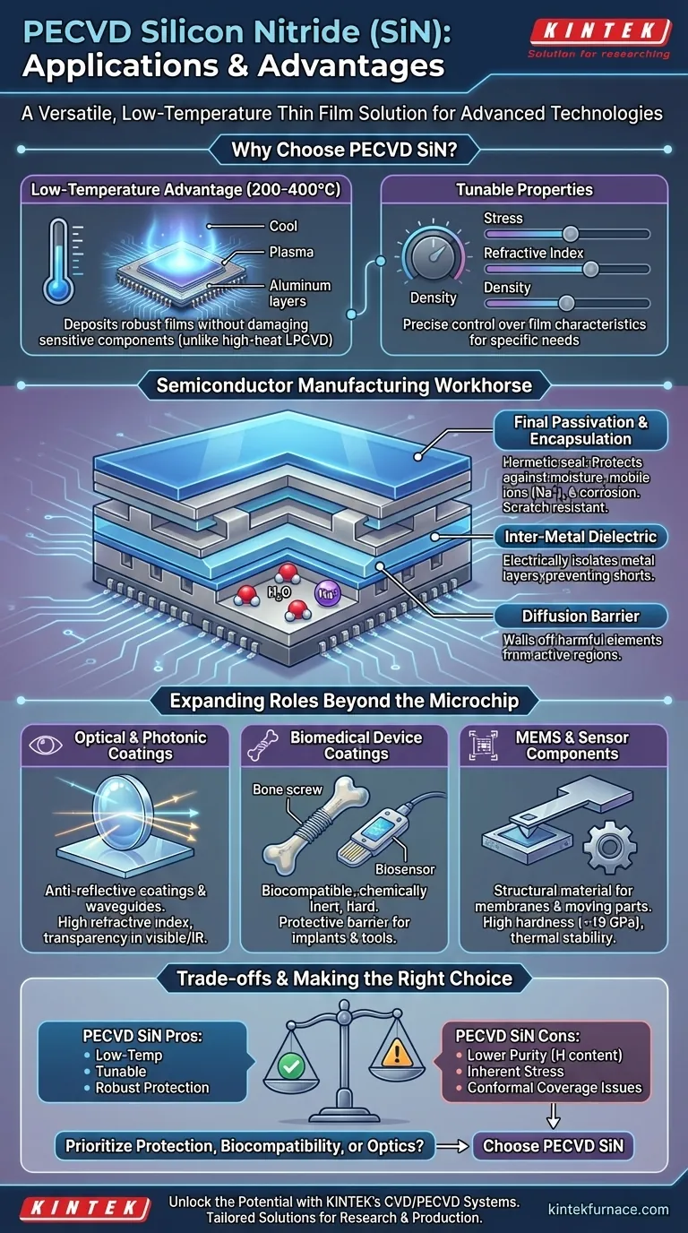
The Foundation: Why Choose PECVD for Silicon Nitride?
Plasma-Enhanced Chemical Vapor Deposition (PECVD) is not the only way to create a Silicon Nitride film, but its specific process characteristics make it uniquely suitable for many modern technologies.
The Low-Temperature Advantage
The defining feature of PECVD is its use of a plasma to energize precursor gases. This allows the chemical reaction that forms the SiN film to occur at much lower temperatures (typically 200-400°C) compared to other methods like Low-Pressure CVD (LPCVD), which can require over 700°C.
This low-temperature budget is critical. It allows SiN to be deposited on top of fully fabricated integrated circuits with sensitive metal layers (like aluminum) that would be destroyed by higher heat.
Tunable Film Properties
The PECVD process offers significant control over the final film's characteristics. By precisely adjusting parameters like gas mixture, pressure, RF power, and temperature, engineers can tune the film's properties.
This includes adjusting the film stress (from compressive to tensile), refractive index, density, and chemical composition to match the specific requirements of the application.
Core Applications in Semiconductor Manufacturing
PECVD SiN is a workhorse material in the fabrication of integrated circuits (ICs), MEMS, and LEDs. Its primary roles are defensive, protecting the delicate device underneath.
Final Passivation and Encapsulation
This is the most common application. A final, thick layer of PECVD SiN is deposited over the completed chip to act as a hermetic seal.
This layer provides robust protection against moisture, mobile ions (like sodium), and other contaminants that could cause corrosion or electrical failure. It also offers a degree of scratch resistance during packaging.
Inter-Metal Dielectric
Within the complex layered structure of an IC, SiN serves as a dielectric insulator. It is used to electrically isolate different metal layers from one another, preventing short circuits and ensuring the integrity of the circuit pathways.
Diffusion Barrier
Silicon Nitride is exceptionally effective at blocking the movement, or diffusion, of certain atoms. It is specifically used as a barrier against water molecules (H₂O) and alkali ions (like Na⁺).
These elements are highly detrimental to semiconductor device performance and reliability, and the SiN layer effectively walls them off from the active regions of the chip.
Expanding Roles Beyond the Microchip
The beneficial properties of PECVD SiN have led to its adoption in several other high-technology fields.
Optical and Photonic Coatings
With a high refractive index and good transparency in the visible and infrared spectra, PECVD SiN is an excellent material for optical coatings.
It is commonly used to create anti-reflective coatings on lenses and solar cells, increasing light transmission and efficiency. It also serves as the core material for waveguides in integrated photonics.
Biomedical Device Coatings
PECVD SiN is biocompatible, chemically inert, and very hard. When coated on medical implants, surgical tools, or biosensors, it acts as a protective barrier.
This coating prevents the device from corroding in the body and isolates the body from potentially reactive materials in the device, ensuring patient safety and device longevity.
MEMS and Sensor Components
Micro-Electro-Mechanical Systems (MEMS) often require materials that are both mechanically strong and stable at various temperatures. PECVD SiN's high hardness (~19 GPa) and thermal stability make it an ideal structural material for membranes, cantilevers, and other moving parts in microscopic sensors and actuators.
Understanding the Trade-offs
While incredibly useful, PECVD SiN is not a perfect solution for every scenario. Understanding its limitations is key to using it effectively.
Film Quality vs. Temperature
The primary trade-off for the low-temperature process is film purity. PECVD SiN incorporates a significant amount of hydrogen into the film, which comes from the precursor gases (like silane and ammonia).
This makes the film less dense and generally lower in quality than the stoichiometric Si₃N₄ produced by high-temperature LPCVD. For applications demanding the absolute highest film purity and density, PECVD may not be the best choice.
Inherent Film Stress
All PECVD films possess an inherent mechanical stress, which can be either compressive (pushing) or tensile (pulling). If this stress is not carefully managed, it can cause the film to crack or even warp the underlying wafer, especially for thicker film depositions.
Conformal Coverage
While good, PECVD's ability to uniformly coat complex, three-dimensional structures (its "conformality") is inferior to other methods like Atomic Layer Deposition (ALD) or LPCVD. For devices with extremely deep, narrow trenches, PECVD may not provide an adequately uniform coating.
Making the Right Choice for Your Application
The decision to use PECVD Silicon Nitride hinges on a clear understanding of your project's priorities.
- If your primary focus is protecting sensitive electronics: Use PECVD SiN for its superior passivation and diffusion barrier capabilities at a device-safe temperature.
- If your primary focus is biocompatibility and durability: Use it as an inert, hard coating for medical devices and implants to ensure long-term stability in a biological environment.
- If your primary focus is optical performance: Leverage its tunable high refractive index and transparency for anti-reflective coatings and photonic waveguides.
- If your primary focus is ultimate film purity and thermal stability: Consider higher-temperature LPCVD, but only if your substrate and underlying device structures can tolerate the heat.
Ultimately, choosing PECVD SiN is a deliberate engineering decision that balances the need for robust protection with the practical constraints of modern manufacturing.
Summary Table:
| Application Area | Key Functions | Key Properties Utilized |
|---|---|---|
| Semiconductor Manufacturing | Passivation, Encapsulation, Dielectric Insulation, Diffusion Barrier | Dielectric, Barrier, Low-Temperature Deposition |
| Optical and Photonic Coatings | Anti-Reflective Coatings, Waveguides | High Refractive Index, Transparency |
| Biomedical Device Coatings | Protective Barrier for Implants and Tools | Biocompatibility, Chemical Inertness, Hardness |
| MEMS and Sensor Components | Structural Material for Membranes and Cantilevers | High Hardness, Thermal Stability |
Unlock the potential of PECVD Silicon Nitride for your advanced applications! At KINTEK, we leverage exceptional R&D and in-house manufacturing to provide diverse laboratories with tailored high-temperature furnace solutions, including our CVD/PECVD Systems. Our strong deep customization capability ensures we precisely meet your unique experimental requirements, whether for semiconductor fabrication, medical device coatings, or optical innovations. Contact us today to discuss how our expertise can enhance your projects and deliver robust, reliable results tailored to your needs.
Visual Guide
Related Products
- Slide PECVD Tube Furnace with Liquid Gasifier PECVD Machine
- Inclined Rotary Plasma Enhanced Chemical Deposition PECVD Tube Furnace Machine
- RF PECVD System Radio Frequency Plasma Enhanced Chemical Vapor Deposition
- Inclined Rotary Plasma Enhanced Chemical Deposition PECVD Tube Furnace Machine
People Also Ask
- What plasma source is used in PE-CVD tube furnaces? Unlock Low-Temperature, High-Quality Deposition
- In which industries is the tube furnace commonly used? Essential for Materials Science, Energy, and More
- What role does a Tube Furnace play in the CVD growth of carbon nanotubes? Achieve High-Purity CNT Synthesis
- What are the typical conditions for plasma-enhanced CVD processes? Achieve Low-Temperature Thin Film Deposition
- How does a hydrogen reduction environment in an industrial tube furnace facilitate gold-copper alloy microspheres?


