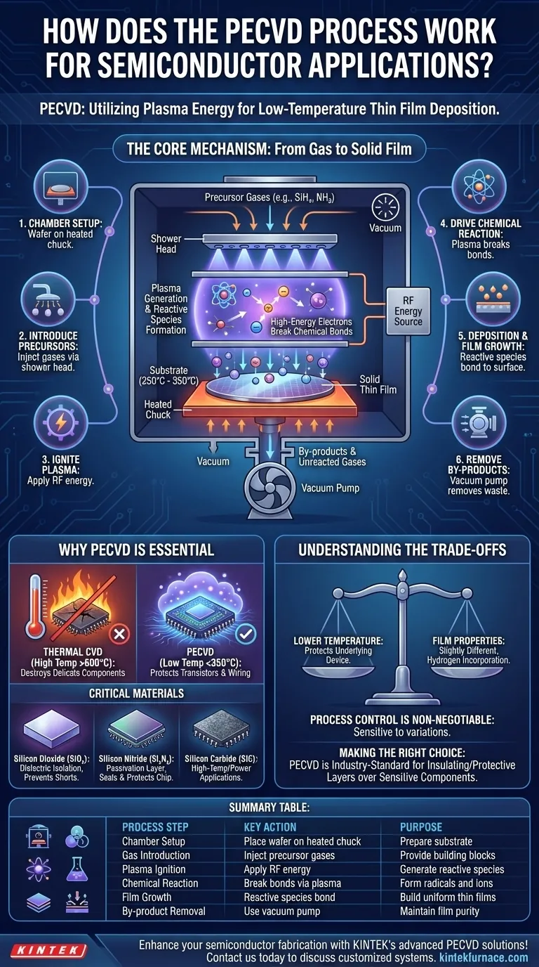
In essence, Plasma-Enhanced Chemical Vapor Deposition (PECVD) works by using an energized plasma to break down precursor gases into reactive species. These species then deposit onto a heated substrate, forming a solid, high-quality thin film. Unlike purely thermal methods, this plasma energy allows the process to occur at much lower temperatures, which is critical for fabricating modern semiconductor devices without damaging their delicate structures.
The fundamental advantage of PECVD is its ability to substitute plasma energy for extreme heat. This solves the critical manufacturing problem of depositing essential insulating and protective films onto a semiconductor wafer after temperature-sensitive components like transistors have already been built.
The Core Mechanism: From Gas to Solid Film
To understand PECVD, it's best to visualize it as a precise, step-by-step assembly line operating at the atomic level within a vacuum chamber.
Setting the Stage in the Chamber
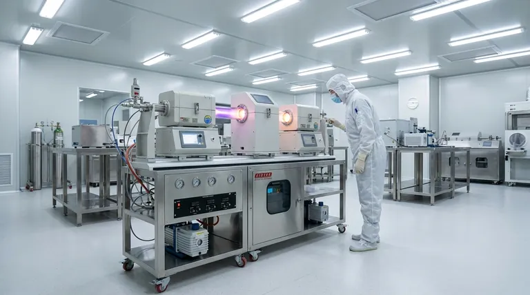
The process begins by placing a semiconductor wafer (the substrate) onto a heated chuck, typically between 250°C and 350°C. This entire assembly is housed within a vacuum chamber situated between two parallel electrodes.
Introducing the Precursors
A carefully controlled mixture of precursor gases is introduced into the chamber, often through a "shower head" for uniform distribution. These gases are the chemical building blocks for the final film, such as silane (SiH₄) and ammonia (NH₃) to create silicon nitride.
Igniting the Plasma
A powerful, high-frequency electrical field (RF energy) is applied across the electrodes. This energy strips electrons from the gas molecules, creating plasma—a highly reactive, glowing state of matter composed of ions, electrons, and neutral species.
Driving the Chemical Reaction
Within the plasma, high-energy electrons collide with the precursor gas molecules. These collisions have enough energy to break the chemical bonds of the precursors, creating a soup of highly reactive chemical fragments (radicals and ions). This step is driven by plasma energy, not just thermal energy.
Deposition and Film Growth
These reactive species are drawn to the surface of the heated wafer. Once there, they bond with the surface and with each other, gradually building up a solid, uniform thin film, one atomic layer at a time.
Removing By-products
Throughout the process, a vacuum pump continuously removes unreacted gases and chemical by-products from the chamber, ensuring the purity and quality of the depositing film.
Why PECVD is Essential for Modern Semiconductors
The true value of PECVD lies in the problems it solves during the complex fabrication of an integrated circuit.
The Low-Temperature Advantage
Traditional Chemical Vapor Deposition (CVD) requires very high temperatures (often >600°C) to thermally break down precursor gases. Such temperatures would destroy or alter the transistors and delicate metal wiring already fabricated on a wafer. PECVD's low-temperature nature makes it the go-to method for deposition steps that occur later in the manufacturing flow.
Critical Materials and Their Roles
PECVD is used to deposit several films that are fundamental to a chip's function and reliability.
- Silicon Dioxide (SiO₂): Used as a dielectric to electrically isolate different conductive layers, preventing short circuits.
- Silicon Nitride (Si₃N₄): Serves as a robust passivation layer, creating a final protective barrier that seals the chip from moisture, mobile ions, and physical damage. This dramatically improves device stability and lifespan.
- Silicon Carbide (SiC): Employed in high-temperature or high-power devices due to its excellent thermal and chemical stability.
Understanding the Trade-offs
While indispensable, PECVD is a process of controlled compromises. Understanding these trade-offs is key to its successful implementation.
Quality vs. Temperature
The defining feature of PECVD is its low-temperature operation. However, films deposited at higher temperatures via thermal processes often have superior properties, such as higher density and lower hydrogen content. The choice of PECVD is an explicit trade-off: accepting slightly different film properties to avoid damaging the underlying device.
Control is Non-Negotiable
The final properties of the film—such as its density, stress, and electrical characteristics—are highly sensitive to process parameters. Small variations in temperature, pressure, gas flow rates, or RF power can significantly alter the outcome, requiring extremely tight process control.
Incorporation of Hydrogen
Because many precursors (like silane) are hydrogen-based, PECVD films inevitably incorporate some hydrogen atoms. While often manageable, this hydrogen can impact the film's electrical properties and long-term stability, a factor engineers must account for in their device design.
Making the Right Choice for Your Goal
Selecting a deposition technique depends entirely on when it is used in the manufacturing sequence and what its primary function is.
- If your primary focus is depositing a foundational layer early in the process (before transistors exist): You might consider a high-temperature thermal CVD process to achieve the highest possible film quality and density.
- If your primary focus is depositing an insulating or protective layer over existing, sensitive components: PECVD is the industry-standard and often the only viable choice due to its low-temperature profile.
- If your primary focus is creating specialized optical or mechanical films (e.g., for LEDs or MEMS): PECVD offers the versatility to tune film properties like refractive index and mechanical stress by adjusting its numerous process parameters.
Ultimately, PECVD is a cornerstone technology that enables the reliable, high-volume production of the complex, multi-layered devices that power our world.
Summary Table:
| Process Step | Key Action | Purpose |
|---|---|---|
| Chamber Setup | Place wafer on heated chuck in vacuum | Prepare substrate for deposition |
| Gas Introduction | Inject precursor gases (e.g., SiH₄, NH₃) | Provide chemical building blocks |
| Plasma Ignition | Apply RF energy to create plasma | Generate reactive species at low temperatures |
| Chemical Reaction | Break bonds in gases via plasma collisions | Form radicals and ions for deposition |
| Film Growth | Reactive species bond to heated substrate | Build uniform solid thin films |
| By-product Removal | Use vacuum pump to extract waste gases | Maintain film purity and quality |
Enhance your semiconductor fabrication with KINTEK's advanced PECVD solutions! Leveraging exceptional R&D and in-house manufacturing, we provide diverse laboratories with high-temperature furnace systems like CVD/PECVD, tailored to your unique needs. Our expertise ensures precise, low-temperature deposition for superior device performance. Contact us today to discuss how our customized PECVD systems can optimize your process and boost efficiency!
Visual Guide
Related Products
- Slide PECVD Tube Furnace with Liquid Gasifier PECVD Machine
- RF PECVD System Radio Frequency Plasma Enhanced Chemical Vapor Deposition
- Inclined Rotary Plasma Enhanced Chemical Deposition PECVD Tube Furnace Machine
- Inclined Rotary Plasma Enhanced Chemical Deposition PECVD Tube Furnace Machine
- Multi Heating Zones CVD Tube Furnace Machine for Chemical Vapor Deposition Equipment
People Also Ask
- What plasma source is used in PE-CVD tube furnaces? Unlock Low-Temperature, High-Quality Deposition
- How does PECVD equipment contribute to TOPCon bottom cells? Mastering Hydrogenation for Maximum Solar Efficiency
- What are the main advantages of PECVD tube furnaces compared to CVD tube furnaces? Lower Temp, Faster Deposition, and More
- What are the typical conditions for plasma-enhanced CVD processes? Achieve Low-Temperature Thin Film Deposition
- What is plasma in the context of PECVD? Unlock Low-Temperature Thin Film Deposition


