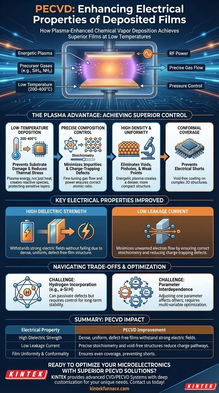
In short, Plasma-Enhanced Chemical Vapor Deposition (PECVD) improves the electrical properties of films by using an energy-rich plasma to precisely control the film's chemical composition, density, and structural integrity at low temperatures. This level of control allows for the creation of highly uniform, dense insulating layers with high dielectric strength and low leakage currents, which are essential for modern microelectronics.
The core advantage of PECVD is not merely the deposition itself, but its function as a highly tunable engineering tool. By manipulating the plasma environment, you can directly engineer the film's atomic structure to achieve specific, superior electrical characteristics that are unattainable with conventional thermal methods.
The Plasma Advantage: How PECVD Achieves Superior Control
The defining feature of PECVD is the use of a plasma to energize precursor gases. This plasma-based process is the direct source of the enhanced electrical properties observed in the resulting films.
Low-Temperature Deposition for Structural Integrity
Traditional Chemical Vapor Deposition (CVD) relies on high temperatures (often >600°C) to break down precursor gases. PECVD, however, uses the energy from the plasma—not just heat—to create reactive species.
This allows for deposition at much lower temperatures (typically 200-400°C). Lower temperatures prevent damage to sensitive underlying device layers and reduce thermal stress, which can create structural defects that degrade electrical performance.
Precise Control Over Film Composition
The electrical behavior of a film, especially an insulator like silicon nitride (SiNx) or silicon dioxide (SiO2), is highly dependent on its exact chemical makeup or stoichiometry.
PECVD provides exceptional control over this by allowing fine-tuning of gas flow rates, pressure, and RF power. This ensures the correct ratio of atoms is deposited, minimizing impurities and charge-trapping defects that would otherwise create pathways for leakage current.
Achieving High Density and Uniformity
A film's ability to insulate is directly tied to its physical structure. Voids, pinholes, or areas of low density act as weak points that can lead to electrical breakdown.
The energetic plasma in a PECVD process helps create a denser, more compact film structure. Process parameters like electrode geometry and chamber pressure are optimized to ensure the film is deposited with excellent uniformity across the entire wafer, eliminating weak spots.
Conformal Coverage on Complex Structures
Modern integrated circuits feature complex, three-dimensional topographies. An insulating layer must cover these features evenly without creating voids or gaps, a property known as conformality.
PECVD excels at producing highly conformal, "void-free" films. This prevents unintended electrical shorts between adjacent conductive layers, a critical requirement for device reliability.
Key Electrical Properties and Their Origins
The process control afforded by PECVD translates directly into measurable improvements in two critical electrical properties.
High Dielectric Strength
Dielectric strength is the maximum electric field an insulating material can withstand without failing and conducting electricity.
A high-quality PECVD film achieves superior dielectric strength because it is dense, uniform, and largely free of defects. With fewer structural weak points to initiate failure, the film can tolerate a much stronger electric field before breaking down.
Low Leakage Current
Leakage current is the small, unwanted flow of electricity through an insulating layer. In microelectronics, this leads to power consumption and device failure.
PECVD minimizes leakage current in two ways. First, by ensuring correct stoichiometry, it reduces the number of chemical defects that can trap and conduct charge. Second, its dense and void-free structure eliminates physical pathways for current to leak through the film.
Understanding the Trade-offs
While powerful, PECVD is not without its complexities. Objectivity requires acknowledging its operational challenges.
The Challenge of Hydrogen Incorporation
Many PECVD processes use hydrogen-containing precursors (like silane, SiH4). As a result, hydrogen is often incorporated into the deposited film (e.g., amorphous silicon, a-Si:H).
While hydrogen can be beneficial for "passivating" or neutralizing certain defects, its presence can also lead to long-term stability issues if not properly controlled.
Parameter Interdependence
A PECVD system has numerous control parameters: RF power, frequency, gas flow rates, pressure, temperature, and electrode spacing.
The primary challenge is that these parameters are highly interdependent. Adjusting one to optimize for a property like stress can inadvertently affect another, like the refractive index or deposition rate. Achieving the desired film requires a complex, multi-variable optimization process.
Making the Right Choice for Your Goal
Your process parameters should be driven by the primary electrical characteristic you need to optimize.
- If your primary focus is maximum insulation (high dielectric strength): You must prioritize process conditions that yield a dense, uniform, and pinhole-free film.
- If your primary focus is minimizing power loss (low leakage current): You must meticulously control gas precursors to achieve perfect stoichiometry and minimize chemical impurities.
- If your primary focus is device passivation: Your goal is a conformal film that blankets the surface and chemically neutralizes defects, often by carefully controlling hydrogen incorporation.
Ultimately, mastering PECVD is about understanding it as a precise instrument for building materials atom-by-atom to meet a specific electrical demand.
Summary Table:
| Electrical Property | How PECVD Improves It |
|---|---|
| High Dielectric Strength | Achieved through dense, uniform, defect-free films that withstand strong electric fields. |
| Low Leakage Current | Minimized by precise stoichiometry control and void-free structures to reduce charge pathways. |
| Film Uniformity and Conformality | Ensures even coverage on complex structures, preventing electrical shorts and enhancing reliability. |
Ready to optimize your microelectronics with superior PECVD solutions? Leveraging exceptional R&D and in-house manufacturing, KINTEK provides diverse laboratories with advanced high-temperature furnace solutions, including CVD/PECVD Systems. Our strong deep customization capability precisely meets your unique experimental needs for enhanced electrical properties. Contact us today to discuss how we can support your goals!
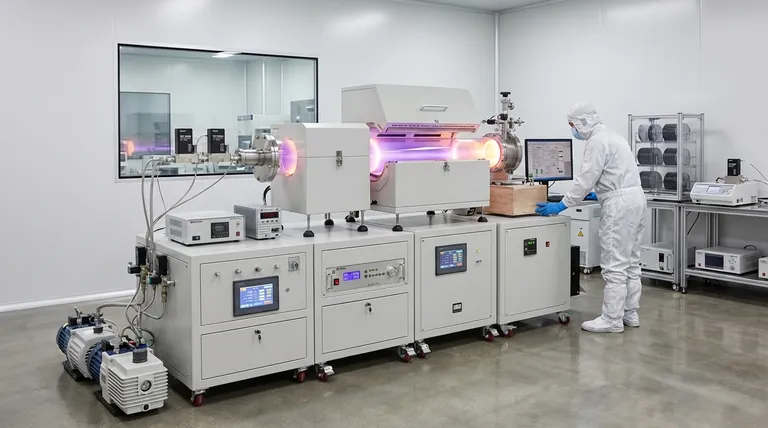
Visual Guide
Related Products
- Slide PECVD Tube Furnace with Liquid Gasifier PECVD Machine
- RF PECVD System Radio Frequency Plasma Enhanced Chemical Vapor Deposition
- Inclined Rotary Plasma Enhanced Chemical Deposition PECVD Tube Furnace Machine
- Inclined Rotary Plasma Enhanced Chemical Deposition PECVD Tube Furnace Machine
- Multi Heating Zones CVD Tube Furnace Machine for Chemical Vapor Deposition Equipment
People Also Ask
- What plasma source is used in PE-CVD tube furnaces? Unlock Low-Temperature, High-Quality Deposition
- How does PECVD equipment contribute to TOPCon bottom cells? Mastering Hydrogenation for Maximum Solar Efficiency
- What are the typical conditions for plasma-enhanced CVD processes? Achieve Low-Temperature Thin Film Deposition
- What is plasma in the context of PECVD? Unlock Low-Temperature Thin Film Deposition
- What are the main advantages of PECVD tube furnaces compared to CVD tube furnaces? Lower Temp, Faster Deposition, and More


