At its core, Chemical Vapor Deposition (CVD) is a material fabrication process that builds a solid, high-purity thin film on a surface from a gas. Unlike simply spraying a coating, CVD involves introducing reactive precursor gases into a controlled chamber where they undergo a chemical reaction on a heated object (the substrate), depositing a new solid layer molecule by molecule.
The critical distinction of CVD is that it does not simply move a material from a source to a target. Instead, it uses gaseous chemical ingredients to synthesize an entirely new, solid material directly onto the substrate's surface, resulting in an exceptionally pure and uniform coating.
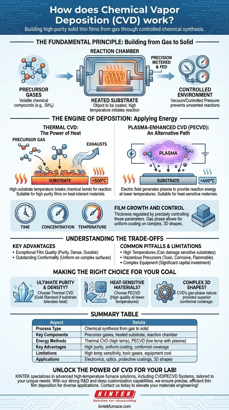
The Fundamental Principle: Building from Gas to Solid
Chemical Vapor Deposition is fundamentally a process of controlled chemical synthesis. It is used when the goal is to create a film with very high quality, purity, and uniformity across a surface.
The Role of Precursors
The process begins with precursor gases. These are volatile chemical compounds that contain the atoms you want to deposit. For example, to create a silicon film, a precursor like silane gas (SiH₄) might be used.
These gases are precisely metered and fed into a sealed reaction chamber.
The Substrate as a Foundation
Inside the chamber is the substrate, which is the object or material to be coated. The substrate is heated to a specific, high temperature, which is critical for initiating the chemical reaction.
The Reaction Chamber: A Controlled Environment
The entire process takes place in a reaction chamber, often under a vacuum or at a controlled pressure. This control is essential to prevent unwanted chemical reactions with air and to manage the behavior of the precursor gases.
The Engine of Deposition: Applying Energy
For the precursor gases to become a solid film, they need an input of energy to break their chemical bonds and react. The method of supplying this energy defines the type of CVD process.
Thermal CVD: The Power of Heat
In the most common method, Thermal CVD, the substrate is heated to hundreds or even thousands of degrees Celsius. When the precursor gases come into contact with this hot surface, the thermal energy forces them to decompose or react.
The resulting solid atoms or molecules then bond to the substrate, building up the thin film. Any gaseous byproducts from the reaction are exhausted from the chamber.
Plasma-Enhanced CVD (PECVD): An Alternative Path
Sometimes, the high temperatures of thermal CVD can damage the substrate. Plasma-Enhanced CVD (PECVD) is a solution that allows deposition at much lower temperatures.
Instead of relying solely on heat, PECVD uses an electric field to generate a plasma—a highly energetic state of gas. This plasma provides the energy to break apart the precursor molecules, allowing the deposition reaction to occur without extreme heat.
Film Growth and Control
The thickness of the deposited film is precisely regulated by controlling the deposition time, the concentration of the precursor gases, and the temperature. Because the precursors are in a gas phase, they can reach and coat all exposed surfaces, even on complex, three-dimensional shapes, with exceptional uniformity.
Understanding the Trade-offs
No single process is perfect for every application. CVD is chosen for its advantages but also has inherent limitations.
Key Advantages of CVD
The primary benefit of CVD is the exceptional quality of the film. It produces coatings that are highly pure, dense, and durable.
Its gas-phase nature also provides outstanding conformality, meaning it can uniformly coat intricate and complex surfaces, unlike line-of-sight methods like sputtering.
Common Pitfalls and Limitations
The high temperatures required for many thermal CVD processes can damage sensitive substrates, such as plastics or certain electronic components.
Additionally, the precursor gases used can be highly toxic, corrosive, or flammable, requiring sophisticated safety and handling protocols. The equipment itself is complex and can represent a significant capital investment.
Making the Right Choice for Your Goal
Selecting the right deposition method depends entirely on the material properties you need and the constraints of your substrate.
- If your primary focus is ultimate film purity and density: Thermal CVD is often the gold standard, provided your substrate can tolerate the high processing temperatures.
- If your primary focus is coating heat-sensitive materials: Plasma-Enhanced CVD (PECVD) is the superior choice, as it achieves high-quality deposition at significantly lower temperatures.
- If your primary focus is uniform coverage on complex 3D shapes: CVD's gas-phase nature provides exceptional conformal coverage that is difficult to achieve with other methods.
By understanding its principles, you can leverage Chemical Vapor Deposition to engineer materials with unparalleled precision and performance.
Summary Table:
| Aspect | Details |
|---|---|
| Process Type | Chemical synthesis from gas to solid |
| Key Components | Precursor gases, heated substrate, reaction chamber |
| Energy Methods | Thermal CVD (high temp), PECVD (low temp with plasma) |
| Key Advantages | High purity, uniform coating, conformal coverage |
| Limitations | High temp sensitivity, toxic gases, equipment cost |
| Applications | Electronics, optics, protective coatings, 3D shapes |
Unlock the power of CVD for your lab! KINTEK specializes in advanced high-temperature furnace solutions, including CVD/PECVD Systems, tailored to your unique needs. With our strong R&D and deep customization capabilities, we ensure precise, efficient thin film deposition for diverse applications. Contact us today to discuss how our expertise can elevate your materials engineering and drive innovation in your projects!
Visual Guide
Related Products
- Custom Made Versatile CVD Tube Furnace Chemical Vapor Deposition CVD Equipment Machine
- Split Chamber CVD Tube Furnace with Vacuum Station CVD Machine
- Multi Heating Zones CVD Tube Furnace Machine for Chemical Vapor Deposition Equipment
- Slide PECVD Tube Furnace with Liquid Gasifier PECVD Machine
- Inclined Rotary Plasma Enhanced Chemical Deposition PECVD Tube Furnace Machine
People Also Ask
- Why are CVD tube furnace sintering systems indispensable for 2D material research and production? Unlock Atomic-Scale Precision
- What is a CVD tube furnace and what is its primary function? Discover Precision Thin-Film Deposition
- How does CVD tube furnace sintering enhance graphene growth? Achieve Superior Crystallinity and High Electron Mobility
- What are the key application fields of CVD tube furnaces? Unlock Precision in Thin-Film Synthesis
- How can integrating CVD tube furnaces with other technologies benefit device fabrication? Unlock Advanced Hybrid Processes


