Thermal treatment in an annealing furnace is the critical post-processing step required to activate the full potential of Indium Selenide thin films. By subjecting the material to high temperatures—specifically 623 K under an Argon gas atmosphere—the process optimizes the film's structural integrity, dramatically improving electrical connectivity and eliminating internal defects.
Core Takeaway: The annealing process transforms a raw Indium Selenide deposition into a high-performance photoanode by fusing nanoparticles and relieving structural stress. This directly results in a stronger photocurrent response and significantly improved long-term device stability.
The Mechanism of Thermal Optimization
To understand why annealing improves performance, we must look at how heat alters the microscopic structure of the material.
Improving Electrical Connectivity
The primary benefit of annealing Indium Selenide is the enhancement of electrical contact between nanoparticles.
During deposition, gaps or poor interfaces often exist between individual particles. High-temperature treatment promotes fusion at these boundaries, creating continuous pathways for electron flow.
Eliminating Residual Stress
Deposition processes often leave thin films with significant internal tension. This residual stress can lead to mechanical instability or poor electronic performance.
Thermal treatment relaxes the material, effectively "healing" the film by releasing this built-up energy.
Optimizing Crystal Quality
Heat provides the energy necessary for atoms to rearrange themselves into a more ordered structure.
This process repairs lattice distortions and optimizes crystal quality. A highly crystalline structure is essential for efficient charge transport, as it reduces the number of defects that can trap electrons.
Impact on Device Performance
The structural changes described above translate directly into measurable performance metrics for photoelectrochemical detectors.
Enhanced Photocurrent Response
Because the electrical contacts are improved and crystal defects are minimized, the film becomes much more efficient at converting light into electrical energy.
This results in a significantly higher photocurrent response, meaning the device generates more power for a given amount of light input.
Superior Long-Term Stability
A film that retains internal stress or structural defects is prone to degradation over time.
By eliminating these stresses and stabilizing the crystal lattice, annealing ensures the device maintains its performance metrics over a longer lifespan, offering better long-term stability.
Understanding the Trade-offs
While annealing is beneficial, it requires precise control over environmental variables to be effective.
Temperature Sensitivity
The specific temperature of 623 K is cited as effective for Indium Selenide.
Deviating significantly from this optimal temperature can be detrimental. Insufficient heat may fail to facilitate nanoparticle contact, while excessive heat could induce material decomposition or unwanted phase changes.
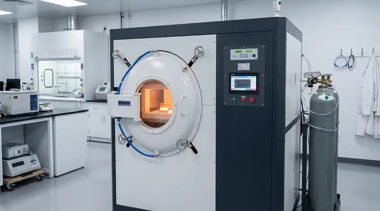
Atmospheric Control
The process relies on an inert atmosphere, such as Argon gas.
Attempting to anneal in an uncontrolled atmosphere (like air) could lead to oxidation, which would degrade the electrical properties of the Indium Selenide rather than improve them.
Optimizing Your Photoanode Process
To achieve the best results with Indium Selenide thin films, your thermal processing strategy should be aligned with your specific performance goals.
- If your primary focus is Maximum Efficiency: Prioritize temperatures that maximize nanoparticle fusion (around 623 K) to ensure the lowest possible electrical resistance.
- If your primary focus is Device Longevity: Ensure the annealing duration is sufficient to fully eliminate residual stress, preventing mechanical failure over time.
Proper annealing is not merely a finishing step; it is the definitive process that stabilizes the material for reliable energy applications.
Summary Table:
| Improvement Factor | Impact of Annealing | Resulting Benefit |
|---|---|---|
| Electrical Contact | Fuses nanoparticles to create continuous pathways | Enhanced electron flow and conductivity |
| Structural Stress | Relaxes internal tension and builds mechanical stability | Increased long-term device durability |
| Crystal Quality | Repairs lattice distortions and reduces trap defects | Significantly higher photocurrent response |
| Atmosphere Control | Prevents oxidation via inert Argon gas environment | Preservation of pure material properties |
Elevate Your Material Research with KINTEK Precision
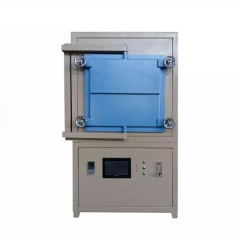
Don't let subpar thermal processing limit your photoanode performance. KINTEK provides the industry-leading laboratory high-temperature furnaces required for delicate thin-film optimization. Backed by expert R&D and world-class manufacturing, we offer a comprehensive range of Muffle, Tube, Rotary, Vacuum, and CVD systems, all of which are fully customizable to meet your unique research needs.
Whether you are refining nanoparticle fusion or eliminating residual stress in advanced semiconductors, our systems deliver the precise temperature and atmospheric control your projects demand. Contact KINTEK today to discuss your specific application and discover how our customizable furnace solutions can drive your next breakthrough.
References
- Yi Xu, Wei Feng. Photoelectrochemical-Type Photodetectors Based on Ball Milling InSe for Underwater Optoelectronic Devices. DOI: 10.3390/nano15010003
This article is also based on technical information from Kintek Furnace Knowledge Base .
Related Products
- Controlled Inert Nitrogen Hydrogen Atmosphere Furnace
- 1400℃ Controlled Inert Nitrogen Atmosphere Furnace
- 1700℃ Controlled Inert Nitrogen Atmosphere Furnace
- Mesh Belt Controlled Atmosphere Furnace Inert Nitrogen Atmosphere Furnace
- 1200℃ Controlled Inert Nitrogen Atmosphere Furnace
People Also Ask
- What are the characteristics and uses of hydrogen atmosphere in furnaces? Achieve Superior Surface Purity and Bonding
- How does a controlled atmosphere furnace contribute to energy efficiency? Lower Costs with Advanced Thermal Management
- Why is a sealed environment important in a controlled atmosphere furnace? Ensure Precision and Safety in High-Temp Processes
- What are the two major categories of controlled atmosphere furnaces? Choose Batch or Continuous for Your Needs
- Mechanism of Fe81Ga19 Secondary Recrystallization? High-Precision Furnace Control for Goss Grain Growth