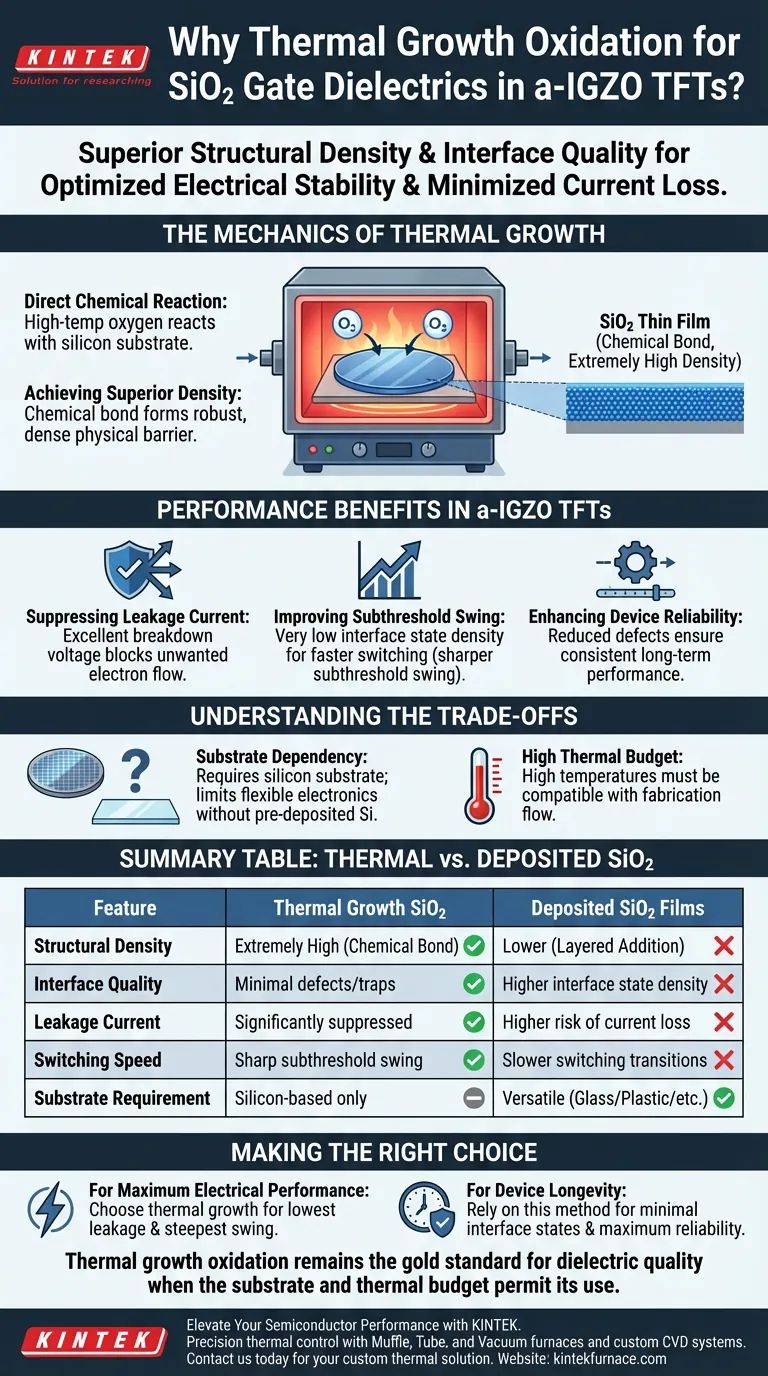
Thermal growth oxidation is the preferred method for preparing Silicon Dioxide (SiO2) gate dielectrics because it yields superior structural density and interface quality. By reacting oxygen directly with a silicon substrate in a high-temperature furnace, this process creates a dielectric layer that outperforms deposited films. For amorphous Indium-Gallium-Zinc Oxide (a-IGZO) Thin-Film Transistors (TFTs), this directly translates to optimized electrical stability and minimized current loss.
Core Takeaway The thermal growth process is not merely a coating technique but a chemical transformation that produces an extremely high-density dielectric with minimal defects. Its primary advantage in a-IGZO TFT applications is the significant suppression of leakage current and the enhancement of device reliability through low interface state density.

The Mechanics of Thermal Growth
Direct Chemical Reaction
Unlike deposition methods that add material on top of a surface, thermal growth involves reacting oxygen directly with the silicon substrate.
This occurs in a high-temperature furnace environment, ensuring a uniform chemical conversion.
Achieving Superior Density
Because the oxide creates a chemical bond with the underlying silicon, the resulting SiO2 thin film possesses extremely high density.
This structural integrity is difficult to replicate with lower-temperature deposition techniques, resulting in a more robust physical barrier.
Performance Benefits in a-IGZO TFTs
Suppressing Leakage Current
The high density of thermally grown SiO2 provides excellent breakdown voltage.
This robust insulation capability effectively blocks unwanted electron flow, significantly suppressing leakage current through the gate dielectric.
Improving Subthreshold Swing
A critical metric for TFT performance is the subthreshold swing, which indicates how quickly a transistor can switch from "off" to "on."
Thermal growth results in very low interface state density, minimizing charge traps that degrade switching speeds. This allows for a sharper, more efficient subthreshold swing.
Enhancing Device Reliability
The reduction in defects and interface traps ensures the device maintains consistent performance over time.
By providing a stable interface for the a-IGZO channel, the thermally grown dielectric improves the overall long-term reliability of the transistor.
Understanding the Trade-offs
Substrate Dependency
This process requires a silicon substrate to react with the oxygen.
It cannot be used on non-silicon substrates (such as glass or plastic) without a pre-deposited silicon layer, limiting its direct application in some flexible electronic contexts.
High Thermal Budget
The process relies on high temperatures to drive the oxidation reaction.
This thermal budget must be compatible with the rest of the fabrication flow. While beneficial for the dielectric quality, it requires careful integration planning to avoid damaging other temperature-sensitive structures.
Making the Right Choice for Your Goal
While thermal growth offers premium quality, it is specific to silicon-based flows.
- If your primary focus is maximum electrical performance: Choose thermal growth to ensure the lowest possible leakage current and steepest subthreshold swing.
- If your primary focus is device longevity: Rely on this method to minimize interface states and maximize the reliability of the a-IGZO TFT.
Thermal growth oxidation remains the gold standard for dielectric quality when the substrate and thermal budget permit its use.
Summary Table:
| Feature | Thermal Growth SiO2 | Deposited SiO2 Films |
|---|---|---|
| Structural Density | Extremely High (Chemical Bond) | Lower (Layered Addition) |
| Interface Quality | Minimal defects/traps | Higher interface state density |
| Leakage Current | Significantly suppressed | Higher risk of current loss |
| Switching Speed | Sharp subthreshold swing | Slower switching transitions |
| Substrate Requirement | Silicon-based only | Versatile (Glass/Plastic/etc.) |
Elevate Your Semiconductor Performance with KINTEK
Precision in dielectric growth starts with superior thermal control. At KINTEK, we empower researchers and manufacturers with high-performance Muffle, Tube, and Vacuum furnaces designed to meet the rigorous thermal budgets of a-IGZO TFT fabrication.
Whether you need customized CVD systems or high-temperature lab furnaces for specialized oxidation processes, our expert R&D and manufacturing teams provide the reliability your innovations demand. Contact us today to find your custom thermal solution and ensure your next project achieves maximum electrical stability and device longevity.
Visual Guide
References
- Sang Yeon Park, Eou‐Sik Cho. 355 nm Nanosecond Ultraviolet Pulsed Laser Annealing Effects on Amorphous In-Ga-ZnO Thin Film Transistors. DOI: 10.3390/mi15010103
This article is also based on technical information from Kintek Furnace Knowledge Base .
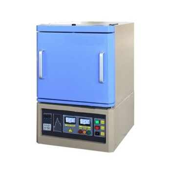
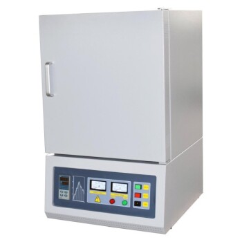
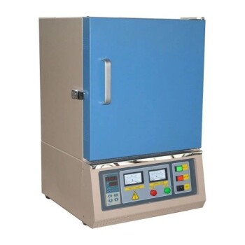
Related Products
- Laboratory Quartz Tube Furnace RTP Heating Tubular Furnace
- Custom Made Versatile CVD Tube Furnace Chemical Vapor Deposition CVD Equipment Machine
- Multi Heating Zones CVD Tube Furnace Machine for Chemical Vapor Deposition Equipment
- Vertical Laboratory Quartz Tube Furnace Tubular Furnace
- 1700℃ High Temperature Laboratory Tube Furnace with Alumina Tube
People Also Ask
- What are the main features and functions of a laboratory tube furnace? Unlock Precise High-Temp Control for Your Lab
- What role does a laboratory tube furnace play in geological and mineralogical research? Unlock Earth's Secrets with Precision
- What conditions do tube furnaces provide for Au-Seeded TiO2 nanowires? Master Precision Thermal Synthesis
- Why is control of heating rate and gas flow in a lab tube furnace critical for EM wave absorption materials?
- What conditions does a tube furnace provide for post-ion-implantation? Achieve Precise Microstructural Repair