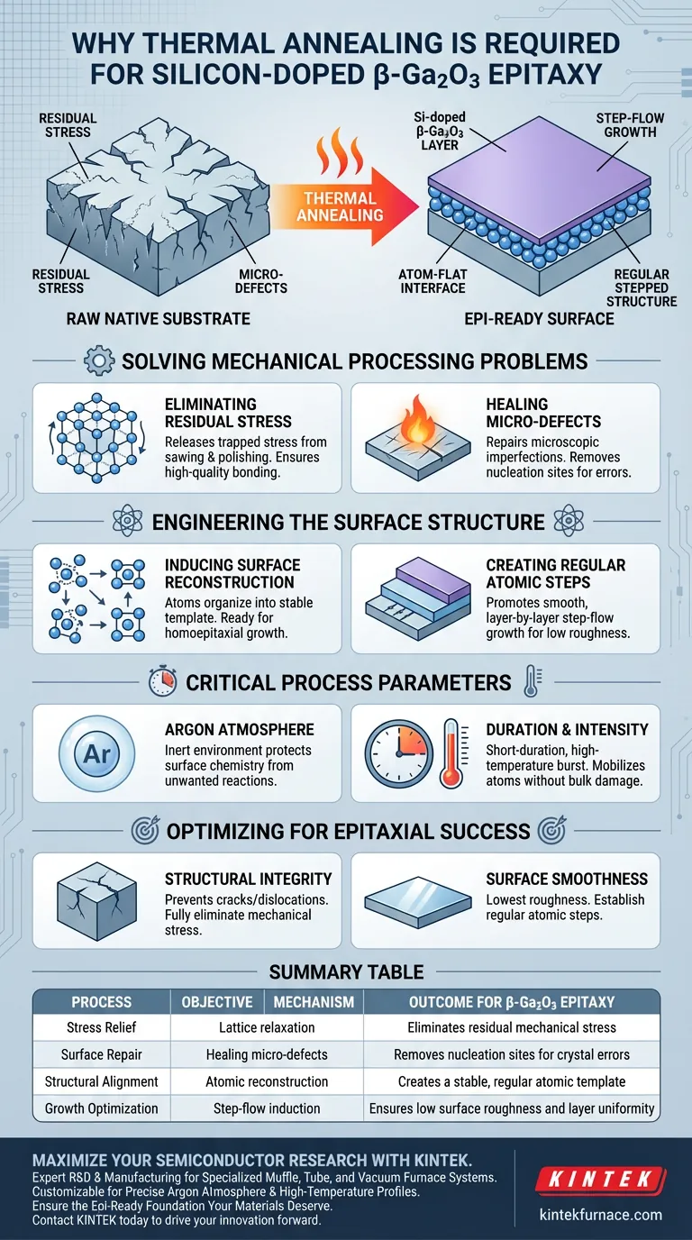
Thermal annealing is the prerequisite step for transforming a raw native substrate into a surface capable of supporting high-quality crystal growth. Before growing silicon-doped beta-gallium oxide ($\beta-Ga_2O_3$), this process is required to repair damage caused by mechanical manufacturing. It reconstructs the atomic surface, creating the stable, "epi-ready" foundation necessary for Metal-Organic Chemical Vapor Deposition (MOCVD).
The core purpose of thermal annealing is to eliminate residual stresses and micro-defects left behind by cutting and polishing. By reorganizing the surface atoms into a regular, stepped structure, annealing ensures the subsequent epitaxial layer is built on a defect-free, atomically flat interface.
Solving the Mechanical Processing Problem
Eliminating Residual Stress
Native substrates undergo significant mechanical processing, such as sawing and polishing, before they reach the growth chamber. These physical forces introduce residual stress into the crystal lattice near the surface.
Without intervention, this stress prevents the formation of a high-quality bond with new layers. Thermal annealing relaxes the lattice, effectively releasing these trapped stresses.
Healing Micro-Defects
Mechanical polishing, while intended to smooth the wafer, often leaves behind microscopic defects and irregularities. These imperfections act as nucleation sites for errors in the new crystal layer.
High-temperature annealing heals these micro-defects. It acts as a corrective reset, returning the surface quality to a state suitable for epitaxy.
Engineering the Surface Structure
Inducing Surface Reconstruction
For successful homoepitaxial growth, the atoms on the substrate surface must be aligned precisely. Annealing induces a process called surface reconstruction.
During this phase, surface atoms shift to find their most energetically stable positions. This creates an organized atomic template that the new silicon-doped $\beta-Ga_2O_3$ layer can replicate.
Creating Regular Atomic Steps
A chaotic surface leads to rough, uneven growth. The annealing process organizes the surface into "regular steps."
These steps promote smooth, layer-by-layer growth (step-flow growth). The result is a surface with extremely low roughness, which is critical for the uniformity of the doped layer.
Critical Process Parameters
The Role of the Argon Atmosphere
The primary reference specifies that this annealing must occur in an argon atmosphere. This inert environment protects the surface chemistry while the heat does its work.
It prevents unwanted chemical reactions or oxidation that could degrade the substrate quality before growth begins.
Duration and Intensity
The process relies on short-duration high-temperature exposure. This burst of thermal energy is sufficient to mobilize surface atoms without damaging the bulk crystal.
This specific thermal profile is calibrated to maximize surface recovery while maintaining the structural integrity of the underlying wafer.
Optimizing for Epitaxial Success
To ensure the best possible performance of your silicon-doped $\beta-Ga_2O_3$ layers, consider how surface preparation impacts your specific goals.
- If your primary focus is Structural Integrity: Prioritize annealing to fully eliminate mechanical stress, preventing cracks or dislocations from propagating into the new layer.
- If your primary focus is Surface Smoothness: Rely on the annealing process to establish regular atomic steps, ensuring the lowest possible roughness for the interface.
A properly annealed substrate is the invisible but non-negotiable guarantor of high-performance semiconductor device layers.
Summary Table:
| Process Objective | Mechanism | Outcome for β-Ga2O3 Epitaxy |
|---|---|---|
| Stress Relief | Lattice relaxation | Eliminates residual mechanical sawing/polishing stress |
| Surface Repair | Healing micro-defects | Removes nucleation sites for crystal errors |
| Structural Alignment | Atomic reconstruction | Creates a stable, regular atomic template |
| Growth Optimization | Step-flow induction | Ensures low surface roughness and layer uniformity |
Maximize Your Semiconductor Research with KINTEK
High-performance $\beta-Ga_2O_3$ devices demand uncompromising substrate preparation. Backed by expert R&D and manufacturing, KINTEK offers specialized Muffle, Tube, and Vacuum furnace systems—all fully customizable to meet the precise argon atmosphere and high-temperature profiles required for your thermal annealing processes.
Whether you are scaling production or refining your epitaxial layers, our precision lab furnaces ensure the "epi-ready" foundation your materials deserve. Contact KINTEK today to discuss your unique lab high-temp furnace needs and see how our expertise can drive your innovation forward.
Visual Guide
References
- D. Gogova, Vanya Darakchieva. High crystalline quality homoepitaxial Si-doped <i>β</i>-Ga2O3(010) layers with reduced structural anisotropy grown by hot-wall MOCVD. DOI: 10.1116/6.0003424
This article is also based on technical information from Kintek Furnace Knowledge Base .
Related Products
- Controlled Inert Nitrogen Hydrogen Atmosphere Furnace
- 1700℃ Controlled Inert Nitrogen Atmosphere Furnace
- 1200℃ Controlled Inert Nitrogen Atmosphere Furnace
- High Temperature Muffle Oven Furnace for Laboratory Debinding and Pre Sintering
- Mesh Belt Controlled Atmosphere Furnace Inert Nitrogen Atmosphere Furnace
People Also Ask
- What are the characteristics and uses of hydrogen atmospheres in furnaces? Unlock Clean Metal Processing
- Mechanism of Fe81Ga19 Secondary Recrystallization? High-Precision Furnace Control for Goss Grain Growth
- Why is controlled atmosphere capability important in an atmosphere furnace? Unlock Precise Material Processing
- What environmental benefits do controlled atmosphere furnaces offer? Reduce Waste and Boost Efficiency
- How does a controlled atmosphere furnace prevent oxidation and decarburization? Master Precision Heat Treatment


