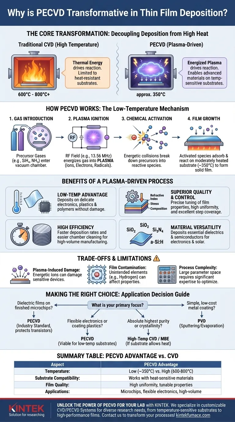
At its core, PECVD is transformative because it decouples the deposition of high-quality thin films from the need for high temperatures. By using an energized plasma to drive chemical reactions instead of intense heat, it allows for advanced materials to be deposited onto temperature-sensitive substrates, opening up fabrication possibilities that were previously impossible with traditional methods like chemical vapor deposition (CVD).
The true innovation of Plasma-Enhanced Chemical Vapor Deposition (PECVD) lies in its use of an energized gas, or plasma, to activate chemical reactions. This fundamental shift allows for the creation of uniform, high-performance films at low temperatures, making it indispensable for modern electronics, optics, and nanotechnology.

How PECVD Bypasses the High-Temperature Barrier
Traditional deposition methods rely on thermal energy—high heat—to break down precursor gases and form a film on a substrate. PECVD circumvents this by creating a highly reactive environment without extreme temperatures.
The Central Role of Plasma
Plasma is often called the fourth state of matter. It is a gas that has been energized, typically by a radio frequency (RF) electric field, causing its atoms and molecules to split into a mix of ions, electrons, and highly reactive neutral species called radicals.
Think of it like this: conventional CVD uses a hot oven to cook ingredients together. PECVD, in contrast, uses a microwave that energizes the ingredients directly, enabling them to react without heating up the entire container.
The Deposition Mechanism
The process occurs within a vacuum chamber at very low pressure.
- Gas Introduction: Precursor gases, such as silane (SiH₄) and ammonia (NH₃) for silicon nitride films, are fed into the chamber.
- Plasma Ignition: An RF electric field (commonly at 13.56 MHz) is applied between two electrodes, igniting the gas and creating a sustained glow discharge—the plasma.
- Chemical Activation: Energetic electrons in the plasma collide with the precursor gas molecules, breaking them down into the reactive ions and radicals needed for film formation.
- Film Growth: These activated species travel to the substrate, which is typically heated to a modest temperature (around 350°C), where they adsorb and react to form a solid, uniform thin film on the surface.
The Low-Temperature Advantage
This process allows for deposition at significantly lower temperatures than conventional CVD, which often requires 600°C to 800°C or higher. This is critical for depositing films on substrates that already contain fabricated electronic components, or on materials like plastics and polymers that would be damaged or destroyed by high heat.
The Benefits of a Plasma-Driven Process
The use of plasma does more than just lower the temperature; it provides a unique level of control and efficiency that makes PECVD a cornerstone of modern manufacturing.
Superior Film Quality and Control
Because the plasma-based reactions are not solely dependent on temperature, technicians gain precise control over film properties. By tuning gas flows, pressure, and RF power, it is possible to engineer the film's refractive index, internal stress, hardness, and chemical composition.
The process also yields films with high uniformity across the entire substrate and excellent step coverage, meaning the film conforms smoothly over the microscopic topography of a device.
High Deposition Rates and Efficiency
PECVD generally achieves higher deposition rates compared to other low-temperature techniques. This, combined with the relative ease of chamber cleaning, makes it a highly efficient and cost-effective method for high-volume manufacturing.
Material Versatility
PECVD is used to deposit a wide range of essential materials, including silicon dioxide (SiO₂), silicon nitride (Si₃N₄), and amorphous silicon (a-Si:H), which are fundamental dielectrics and semiconductors in the electronics and solar industries.
Understanding the Trade-offs and Limitations
While transformative, PECVD is not a universal solution. Understanding its limitations is key to using it effectively.
Potential for Plasma-Induced Damage
The same energetic ions that drive the reaction can also physically bombard the substrate. On highly sensitive devices, this ion bombardment can introduce defects or damage the underlying material, a factor that must be carefully managed by tuning the process parameters.
Film Contamination
Precursor gases often contain elements that are not intended for the final film, most notably hydrogen from precursors like silane (SiH₄). This hydrogen can become incorporated into the film, affecting its electrical and optical properties. While sometimes desirable, it is often a source of contamination that must be controlled.
Process Complexity
The physics and chemistry inside a PECVD chamber are complex. The interplay between gas flow, pressure, temperature, and plasma power creates a large parameter space. Finding the optimal recipe for a specific film can require significant experimentation and expertise.
Making the Right Choice for Your Application
Selecting a deposition technique depends entirely on your project's constraints and goals. PECVD's unique capabilities make it the ideal choice for specific, high-value applications.
- If your primary focus is depositing dielectric films on finished microchips: PECVD is the industry standard, as its low temperature protects the delicate transistors already built on the wafer.
- If your primary focus is creating flexible electronics or coating plastics: PECVD is one of the few viable methods for depositing high-quality inorganic films on low-temperature polymer substrates.
- If your primary focus is the absolute highest film purity or crystallinity: You might need a high-temperature method like traditional CVD or molecular beam epitaxy, assuming your substrate can withstand the heat.
- If your primary focus is a simple, low-cost metal coating: A physical vapor deposition (PVD) technique like sputtering or evaporation may be a more straightforward solution.
By understanding the fundamental advantage of its plasma-driven, low-temperature process, you can leverage PECVD to solve challenges previously limited by thermal constraints.
Summary Table:
| Aspect | PECVD Advantage |
|---|---|
| Temperature | Low-temperature deposition (e.g., ~350°C) vs. high temperatures in CVD (600-800°C) |
| Substrate Compatibility | Works with temperature-sensitive materials like plastics and polymers |
| Film Quality | High uniformity, step coverage, and tunable properties (e.g., refractive index, stress) |
| Applications | Ideal for microchips, flexible electronics, and dielectric films in high-volume manufacturing |
| Limitations | Potential plasma-induced damage, hydrogen contamination, and process complexity |
Unlock the Power of PECVD for Your Lab
At KINTEK, we specialize in advanced high-temperature furnace solutions, including our CVD/PECVD Systems, designed to meet the unique demands of diverse laboratories. Leveraging exceptional R&D and in-house manufacturing, we offer deep customization to precisely address your experimental needs—whether you're working with temperature-sensitive substrates or require high-performance thin films for electronics, optics, or nanotechnology.
Our product line, featuring Muffle, Tube, Rotary Furnaces, Vacuum & Atmosphere Furnaces, and CVD/PECVD Systems, ensures you achieve superior deposition results with enhanced efficiency and control. Don't let thermal constraints limit your innovation—contact us today to discuss how KINTEK can transform your thin film processes and drive your research forward!
Visual Guide
Related Products
- Slide PECVD Tube Furnace with Liquid Gasifier PECVD Machine
- RF PECVD System Radio Frequency Plasma Enhanced Chemical Vapor Deposition
- Inclined Rotary Plasma Enhanced Chemical Deposition PECVD Tube Furnace Machine
- Inclined Rotary Plasma Enhanced Chemical Deposition PECVD Tube Furnace Machine
- Multi Heating Zones CVD Tube Furnace Machine for Chemical Vapor Deposition Equipment
People Also Ask
- How does a hydrogen reduction environment in an industrial tube furnace facilitate gold-copper alloy microspheres?
- What are the disadvantages of tube furnace cracking when processing heavy raw materials? Avoid Costly Downtime and Inefficiency
- What is plasma in the context of PECVD? Unlock Low-Temperature Thin Film Deposition
- In which industries is the tube furnace commonly used? Essential for Materials Science, Energy, and More
- What are the advantages of using a tube furnace CVD system for Cu(111)/graphene? Superior Scalability and Quality


