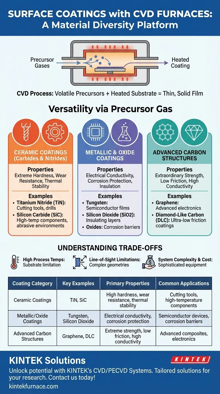
CVD furnaces can deposit an exceptionally broad range of surface coatings, fundamentally altering the properties of a component's surface. These materials fall into major classes including hard ceramics like nitrides and carbides, pure metals and their oxides, and advanced carbon structures like graphene. This versatility allows the process to be tailored for applications ranging from industrial cutting tools to advanced semiconductor devices.
Chemical Vapor Deposition (CVD) is not a single type of coating but a versatile deposition platform. The true value lies in understanding which class of material—ceramic, metallic, or carbon—solves your specific engineering challenge, whether it's enhancing hardness, conductivity, or another key performance metric.
The Foundation: How CVD Enables Material Diversity
The CVD Process in Brief
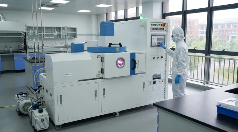
Chemical Vapor Deposition is a process performed in a vacuum chamber where a substrate (the part to be coated) is exposed to one or more volatile chemical precursors. These gaseous precursors decompose or react on the hot substrate's surface, depositing a thin, solid film.
This atom-by-atom or molecule-by-molecule deposition creates a highly pure, dense, and durable coating. Because the film is grown directly on the surface, it forms a strong bond without needing a separate curing step.
Why the Process Allows for Variety
The key to CVD's versatility is the precursor gas. By carefully selecting and controlling the gases introduced into the furnace, engineers can deposit a vast array of different materials. The final coating is determined entirely by the chemical reaction that occurs on the part's surface.
A Breakdown of Key Coating Categories
The coatings achievable with CVD are best understood by their material class and the functional properties they impart.
Ceramic Coatings (Carbides and Nitrides)
These materials are known for their exceptional hardness, wear resistance, and thermal stability. They are the go-to choice for protecting components in high-stress, high-temperature environments.
Common examples include:
- Titanium Nitride (TiN): A gold-colored coating widely used on cutting tools and drills to increase tool life and reduce friction.
- Silicon Carbide (SiC): An extremely hard and corrosion-resistant ceramic used in high-temperature applications and for components exposed to abrasive materials.
Metallic and Oxide Coatings
CVD is also used to deposit highly pure metal films and stable metal oxides. These layers serve entirely different functions than ceramics, often related to electrical or chemical properties.
These coatings are critical for:
- Semiconductor Devices: Depositing conductive metal films like tungsten or insulating oxide layers (e.g., silicon dioxide) is fundamental to manufacturing microchips.
- Corrosion Protection: Applying a dense, non-reactive oxide layer can create an effective barrier against harsh chemical environments.
Advanced Carbon Structures
At the cutting edge of material science, CVD is the primary method for synthesizing advanced forms of carbon, each with extraordinary properties.
Two prominent examples are:
- Graphene: A single-atom-thick sheet of carbon with unparalleled strength and electrical conductivity, used in advanced composites and electronics.
- Diamond and Diamond-Like Carbon (DLC): CVD can grow actual diamond films for extreme hardness or create DLC coatings that offer an incredibly low coefficient of friction.
Understanding the Trade-offs
While powerful, CVD is not a universal solution. Understanding its limitations is critical for making an informed decision.
High Process Temperatures
Traditional CVD processes often require very high temperatures to initiate the necessary chemical reactions on the substrate. This can limit the types of materials that can be coated, as the substrate itself must be able to withstand the heat without deforming or melting.
Line-of-Sight Limitations
In its basic form, CVD is a line-of-sight process, meaning it coats surfaces that are directly exposed to the precursor gas flow. Coating complex, non-line-of-sight geometries or internal channels can be challenging and may require specialized equipment and process development.
System Complexity and Cost
CVD furnaces are sophisticated systems that operate under vacuum with precise control over temperature, pressure, and gas flow. This complexity, along with the cost of precursor gases, can make the process more expensive than some alternative coating methods like painting or electroplating.
Selecting the Right CVD Coating for Your Application
Your choice of coating depends entirely on the problem you need to solve. Use the primary function as your guide.
- If your primary focus is extreme wear resistance and hardness: Ceramic coatings like Titanium Nitride (TiN) and Silicon Carbide (SiC) are the industry standard for tools and mechanical components.
- If your primary focus is electrical functionality or corrosion protection: Explore metallic films for conductivity or stable oxide layers for insulation and chemical resistance.
- If your primary focus is cutting-edge, high-performance properties: Investigate advanced carbon structures like Diamond-Like Carbon (DLC) for ultra-low friction or graphene for next-generation composites.
By matching the material class to your specific goal, you can leverage CVD as a strategic tool for advanced material engineering.
Summary Table:
| Coating Category | Key Examples | Primary Properties | Common Applications |
|---|---|---|---|
| Ceramic Coatings | TiN, SiC | High hardness, wear resistance, thermal stability | Cutting tools, high-temperature components |
| Metallic/Oxide Coatings | Tungsten, Silicon Dioxide | Electrical conductivity, corrosion protection | Semiconductor devices, corrosion barriers |
| Advanced Carbon Structures | Graphene, DLC | Extreme strength, low friction, high conductivity | Advanced composites, electronics |
Unlock the full potential of your laboratory with KINTEK's advanced CVD furnace solutions! Leveraging exceptional R&D and in-house manufacturing, we provide high-temperature furnaces like CVD/PECVD Systems tailored to your unique experimental needs. Our deep customization capabilities ensure precise performance for applications in ceramics, metals, and carbon coatings. Contact us today to discuss how we can enhance your research and development processes!
Visual Guide
Related Products
- Custom Made Versatile CVD Tube Furnace Chemical Vapor Deposition CVD Equipment Machine
- Split Chamber CVD Tube Furnace with Vacuum Station CVD Machine
- Multi Heating Zones CVD Tube Furnace Machine for Chemical Vapor Deposition Equipment
- Slide PECVD Tube Furnace with Liquid Gasifier PECVD Machine
- Controlled Inert Nitrogen Hydrogen Atmosphere Furnace
People Also Ask
- What is a CVD tube furnace and what is its primary function? Discover Precision Thin-Film Deposition
- What improvements can be made to the bonding force of gate dielectric films using a CVD tube furnace? Enhance Adhesion for Reliable Devices
- What future trends are expected in the development of CVD tube furnaces? Discover Smarter, More Versatile Systems
- How does CVD tube furnace sintering enhance graphene growth? Achieve Superior Crystallinity and High Electron Mobility
- What are the key features of CVD tube furnaces for 2D material processing? Unlock Precision Synthesis for Superior Materials


