In short, Chemical Vapor Deposition (CVD) is an exceptionally versatile technique capable of producing a vast spectrum of materials. It can deposit everything from simple metals and alloys to complex semiconductors, advanced ceramics, and revolutionary carbon nanostructures like graphene and synthetic diamond. This flexibility makes CVD a cornerstone technology in industries ranging from microelectronics to aerospace.
The power of CVD lies not just in the materials it can create, but in how it creates them. By using chemical reactions at the molecular level, it allows for the controlled growth of ultra-pure, high-performance thin films and complex structures that are often impossible to produce by other means.
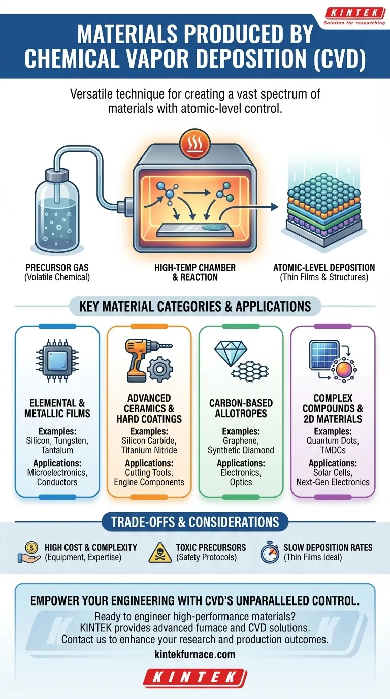
How CVD Achieves Such Versatility
The core of CVD's adaptability is its fundamental process. It doesn't melt and cast material; it builds it from the ground up using a gas.
The Deposition Process
A volatile chemical compound, known as a precursor gas, is introduced into a high-temperature reaction chamber. This heat causes the gas to react or decompose, and the resulting solid material is deposited onto a substrate, layer by layer.
Control at the Atomic Level
Because the material builds up atom by atom, engineers have precise control over its thickness, purity, and crystal structure. By simply changing the precursor gases, temperature, or pressure, an entirely different material can be produced in the same equipment.
A Breakdown of Key Material Categories
The range of materials achievable with CVD is extensive, serving nearly every field of modern technology.
Elemental and Metallic Films
CVD is widely used to deposit high-purity elemental layers. These are fundamental to the semiconductor industry.
Examples include silicon (the basis of most computer chips), tungsten, tantalum, and rhenium. These films serve as conductors, barriers, and structural components in microelectronics.
Advanced Ceramics and Hard Coatings
CVD excels at creating extremely hard, corrosion-resistant, and heat-tolerant ceramic films.
This category includes carbides (e.g., silicon carbide, tungsten carbide), nitrides (e.g., titanium nitride), and oxides (e.g., alumina, zirconia). These coatings are applied to cutting tools, engine components, and industrial equipment to dramatically extend their lifespan.
Carbon-Based Allotropes
Some of the most advanced materials known are produced using specialized CVD processes.
This includes synthetic diamond films, valued for their hardness and optical clarity, as well as graphene and carbon nanotubes, which are two-dimensional and one-dimensional materials with revolutionary electronic and mechanical properties.
Complex Compounds and 2D Materials
Beyond simple elements, CVD can synthesize complex compounds and next-generation materials.
Examples include quantum dots for advanced solar cells and medical imaging, as well as transition metal dichalcogenides (TMDCs), which are another class of 2D materials being explored for next-generation electronics and optics.
Understanding the Trade-offs
While powerful, CVD is not a universal solution. It requires a significant investment in equipment and expertise.
Process Complexity
CVD systems often require high vacuum and very high temperatures, making the equipment expensive to acquire and operate. Precise control over gas flow, temperature, and pressure is critical for achieving uniform, high-quality results.
Precursor Handling
The precursor chemicals used in CVD can be highly toxic, flammable, or corrosive. This necessitates stringent safety protocols and specialized handling infrastructure, adding to the operational complexity and cost.
Deposition Rates
Compared to some other coating methods like physical vapor deposition (PVD) or electroplating, CVD can have relatively slow deposition rates. This makes it ideal for thin, high-performance films but less practical for depositing very thick bulk layers.
Applying This to Your Goal
The right material depends entirely on the problem you need to solve.
- If your primary focus is microelectronics: You will rely on CVD for depositing ultra-pure silicon, tungsten, and dielectric films like silicon dioxide.
- If your primary focus is wear resistance: You will use CVD to apply hard ceramic coatings like titanium nitride or tungsten carbide to tools and mechanical parts.
- If your primary focus is advanced research: You will explore CVD to synthesize cutting-edge materials like graphene, carbon nanotubes, or quantum dots for next-generation devices.
- If your primary focus is optics or harsh environments: You can use CVD to create protective diamond films for windows or coat components with inert metals like iridium.
Ultimately, the unparalleled control offered by CVD empowers you to engineer materials with properties tailored to your specific application.
Summary Table:
| Material Category | Examples | Key Applications |
|---|---|---|
| Elemental and Metallic Films | Silicon, Tungsten, Tantalum | Microelectronics, Conductors |
| Advanced Ceramics and Hard Coatings | Silicon Carbide, Titanium Nitride | Cutting Tools, Engine Components |
| Carbon-Based Allotropes | Graphene, Synthetic Diamond | Electronics, Optics |
| Complex Compounds and 2D Materials | Quantum Dots, TMDCs | Solar Cells, Next-Gen Electronics |
Ready to engineer high-performance materials with precision? Leveraging exceptional R&D and in-house manufacturing, KINTEK provides diverse laboratories with advanced high-temperature furnace solutions. Our product line, including Muffle, Tube, Rotary Furnaces, Vacuum & Atmosphere Furnaces, and CVD/PECVD Systems, is complemented by our strong deep customization capability to precisely meet unique experimental requirements. Contact us today to discuss how our CVD solutions can enhance your research and production outcomes!
Visual Guide
Related Products
- HFCVD Machine System Equipment for Drawing Die Nano Diamond Coating
- Custom Made Versatile CVD Tube Furnace Chemical Vapor Deposition CVD Equipment Machine
- 915MHz MPCVD Diamond Machine Microwave Plasma Chemical Vapor Deposition System Reactor
- Multi Heating Zones CVD Tube Furnace Machine for Chemical Vapor Deposition Equipment
- MPCVD Machine System Reactor Bell-jar Resonator for Lab and Diamond Growth
People Also Ask
- What is Hot-filament Chemical Vapor Deposition (HFCVD)? Achieve High-Quality Thin Films with Precision Control
- What is the function of high-purity Argon (Ar) gas during CVD? Optimize Your Thin Film Uniformity and Purity
- What core function does CVD equipment serve in h-BN anti-corrosion? Master Precision Synthesis for High-Performance Films
- What is the significance of the vacuum pressure control system in the CVD coating process for powders?
- How can customers maximize the quality of CVD coatings? Master Pre-Coating Prep for Superior Results