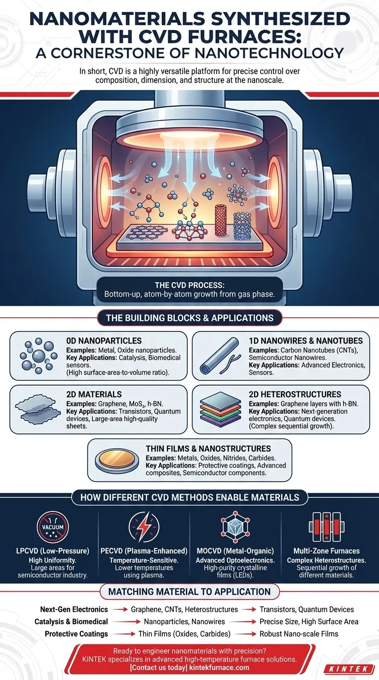
In short, CVD furnaces are a cornerstone of modern nanotechnology. They are used to synthesize a diverse array of nanomaterials, including one-dimensional structures like carbon nanotubes and nanowires, two-dimensional materials such as graphene, and zero-dimensional nanoparticles. The process also extends to complex 2D heterostructures and various nano-scale films, including metals, oxides, nitrides, and carbides.
Chemical Vapor Deposition (CVD) is not just a method for creating a few specific materials; it's a highly versatile platform technology. Its true power lies in the precise control it offers over material composition, dimension, and structure at the nanoscale, enabling the fabrication of advanced materials for next-generation devices.
The Scope of CVD in Nanomaterial Synthesis
The value of CVD comes from its ability to "grow" materials atom-by-atom from a gas phase onto a substrate. This bottom-up approach provides unparalleled control over the final product's properties.
The Building Blocks: From 0D to 2D Materials
CVD can produce nanomaterials across all dimensionalities.
Zero-dimensional (0D) nanoparticles can be synthesized for applications in catalysis and biomedicine, where their high surface-area-to-volume ratio is critical.
One-dimensional (1D) materials are a major strength of CVD. This includes high-purity carbon nanotubes (CNTs) and various metallic or semiconducting nanowires, which are fundamental to advanced electronics and sensors.
Two-dimensional (2D) materials represent a frontier of materials science. CVD is the primary method for producing large-area, high-quality sheets of graphene, as well as other 2D materials like molybdenum disulfide (MoS₂) and hexagonal boron nitride (h-BN).
A Broad Chemical Palette
While carbon-based materials like graphene and CNTs are famous examples, CVD is not limited to them.
The technique is routinely used to deposit thin films and nanostructures of a wide range of inorganic compounds, including metals, oxides, nitrides, and carbides. This versatility makes it essential for creating everything from semiconductor components to durable, protective coatings.
Control Over Form and Function
The most significant advantage of CVD is the ability to tune the final material's properties. By carefully managing process parameters like temperature, pressure, and gas flow, researchers can achieve controllable morphology and size.
This precision is what allows for the creation of materials engineered for specific functions, from electronic band gaps in transistors to active sites on a catalyst.
How Different CVD Methods Enable Different Materials
Not all CVD is the same. Different variations of the core process are used to optimize the synthesis of specific nanomaterials.
LPCVD for High Uniformity
Low-Pressure CVD (LPCVD) operates in a vacuum, which allows precursor gases to diffuse more evenly. This results in highly uniform films over large areas, a critical requirement for the semiconductor industry.
PECVD for Temperature-Sensitive Substrates
Plasma-Enhanced CVD (PECVD) uses an energy-rich plasma to help break down the precursor gases. This allows deposition to occur at much lower temperatures, making it possible to coat materials that cannot withstand the heat of traditional CVD.
MOCVD for Advanced Optoelectronics
Metal-Organic CVD (MOCVD) uses specialized metal-organic precursors to deposit extremely high-purity crystalline films. This technique is indispensable for manufacturing high-performance LEDs and other optoelectronic devices.
Multi-Zone Furnaces for Complex Heterostructures
Advanced CVD systems, such as multi-zone tube furnaces, enable the sequential growth of different materials. This is how 2D heterostructures (e.g., graphene layered with h-BN) are built, creating novel materials for next-generation transistors and quantum devices.
Understanding the Trade-offs and Limitations
While powerful, CVD is not without its challenges. Success depends on navigating key technical constraints.
Precursor and Substrate Compatibility
The entire process hinges on having a suitable precursor gas that will decompose cleanly at a specific temperature. The substrate must also be able to withstand the process conditions and be compatible with the material being grown.
Process Complexity and Cost
Simpler methods like Atmospheric Pressure CVD (APCVD) are faster and cheaper but may yield lower-quality materials. Highly specialized techniques like MOCVD produce exceptional quality but require expensive equipment and rigorous process control.
Contamination and Purity
The final nanomaterial's quality is directly tied to the purity of the precursor gases and the integrity of the reaction chamber. Even minute leaks or impurities can introduce defects, compromising the material's performance.
Matching the Material to Your Application
Your choice of CVD-grown material is dictated entirely by your end goal.
- If your primary focus is next-generation electronics: You will likely use CVD to create high-purity graphene, carbon nanotubes, or complex 2D heterostructures for transistors and quantum devices.
- If your primary focus is catalysis or biomedical sensors: You will leverage CVD to synthesize nanoparticles and nanowires with precisely controlled size and high surface area.
- If your primary focus is protective coatings or advanced composites: You will use CVD to deposit robust nano-scale films of materials like diamond-like carbon, ceramics, nitrides, or carbides.
Ultimately, the versatility of CVD allows you to engineer materials from the atom up, making it an indispensable tool for targeted innovation.
Summary Table:
| Nanomaterial Type | Examples | Key Applications |
|---|---|---|
| 0D Nanoparticles | Metal, oxide nanoparticles | Catalysis, biomedical sensors |
| 1D Nanowires | Carbon nanotubes, semiconductor nanowires | Electronics, advanced sensors |
| 2D Materials | Graphene, MoS₂, h-BN | Transistors, quantum devices |
| Thin Films | Oxides, nitrides, carbides | Protective coatings, composites |
| Heterostructures | Graphene-h-BN layers | Next-generation electronics |
Ready to engineer nanomaterials with precision? KINTEK specializes in advanced high-temperature furnace solutions, including CVD/PECVD systems, tailored for diverse laboratory needs. Leveraging our exceptional R&D and in-house manufacturing, we offer deep customization to meet your unique experimental requirements. Contact us today to discuss how our Muffle, Tube, Rotary, Vacuum & Atmosphere Furnaces, and CVD/PECVD Systems can accelerate your innovation in electronics, catalysis, and beyond!
Visual Guide
Related Products
- Custom Made Versatile CVD Tube Furnace Chemical Vapor Deposition CVD Equipment Machine
- Split Chamber CVD Tube Furnace with Vacuum Station CVD Machine
- Multi Heating Zones CVD Tube Furnace Machine for Chemical Vapor Deposition Equipment
- Slide PECVD Tube Furnace with Liquid Gasifier PECVD Machine
- Controlled Inert Nitrogen Hydrogen Atmosphere Furnace
People Also Ask
- What customization options are available for CVD tube furnaces? Tailor Your System for Superior Material Synthesis
- What future trends are expected in the development of CVD tube furnaces? Discover Smarter, More Versatile Systems
- What is the working principle of a CVD tube furnace? Achieve Precise Thin Film Deposition for Your Lab
- Why are CVD tube furnace sintering systems indispensable for 2D material research and production? Unlock Atomic-Scale Precision
- What are the key features of CVD tube furnaces for 2D material processing? Unlock Precision Synthesis for Superior Materials


