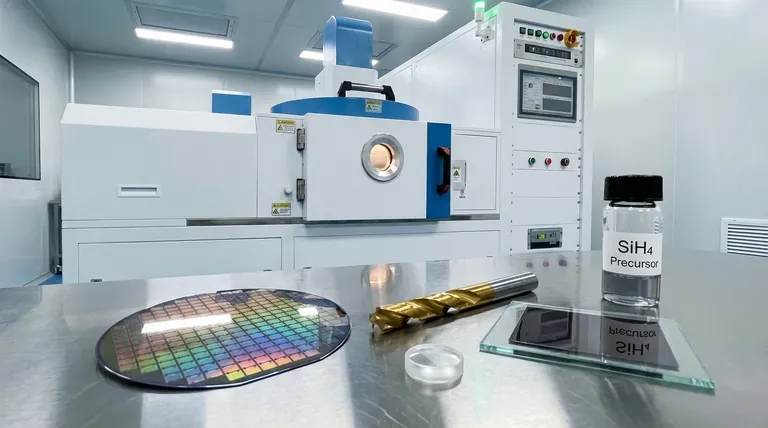
In short, Chemical Vapor Deposition (CVD) can deposit an exceptionally wide range of materials. This includes foundational electronic materials like silicon, insulators such as silicon dioxide, conductive metals like tungsten, and ultra-hard coatings like titanium nitride and diamond-like carbon. The process is so versatile it is also used to create advanced structures like carbon nanotubes and quantum dots.
Chemical Vapor Deposition is not just a single technique but a family of processes defined by their remarkable versatility. Its true power lies in the ability to precisely control the growth of thin films, enabling the creation of materials with tailored electronic, mechanical, or optical properties that are fundamental to virtually all modern high-technology industries.
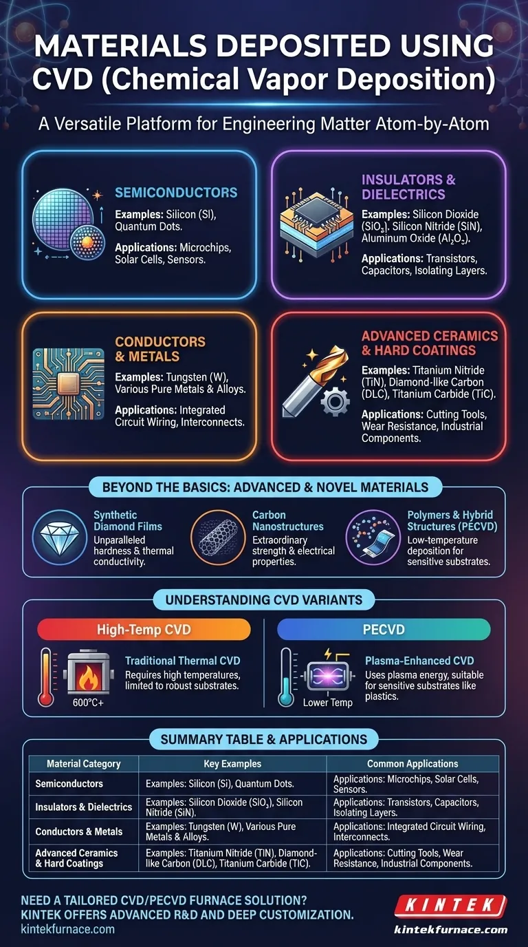
The Fundamental Material Categories of CVD
CVD's flexibility comes from its use of various chemical precursors and energy sources (like heat or plasma) to deposit materials atom-by-atom. This allows for the creation of materials across several critical categories.
Semiconductors
Semiconductors are the bedrock of the electronics industry. CVD is the dominant method for producing the high-purity films required.
Key examples include silicon (Si), in both its amorphous and crystalline forms, which is the foundational material for microchips. CVD is also used to create advanced semiconductor structures like quantum dots for solar cells and medical imaging.
Insulators and Dielectrics
To build a functional electronic device, you must isolate conductive components from one another. CVD excels at depositing high-quality, uniform insulating layers.
Common materials include silicon dioxide (SiO₂) and silicon nitride (SiN), which are essential dielectrics in transistors and capacitors. Aluminum oxide (Al₂O₃) is another key insulator deposited via CVD for various applications.
Conductors and Metals
CVD can also deposit pure metals and conductive compounds, which serve as the "wiring" inside integrated circuits and other devices.
Tungsten (W) is a primary example, used to create robust connections between different layers of a microchip. Other pure metals and alloys can also be deposited depending on the specific process chemistry.
Advanced Ceramics and Hard Coatings
One of the most widespread industrial uses of CVD is for creating extremely hard, durable, and corrosion-resistant coatings.
Materials like titanium nitride (TiN), titanium carbide (TiC), and titanium carbonitride (TiCN) provide exceptional wear resistance for cutting tools and industrial components. Diamond-like carbon (DLC) is another popular coating used to reduce friction and increase the lifespan of mechanical parts.
Beyond the Basics: Advanced and Novel Materials
The adaptability of CVD processes allows researchers and engineers to construct materials with unique and powerful properties that go beyond traditional categories.
Synthetic Diamond Films
Beyond just "diamond-like" carbon, CVD can be used to grow films of pure, synthetic diamond. These films possess unparalleled hardness and thermal conductivity, making them ideal for high-performance cutting tools, durable optical windows, and advanced electronic devices.
Carbon Nanostructures
CVD is a key method for synthesizing advanced carbon forms like carbon nanotubes. These structures have extraordinary strength and unique electrical properties, making them a focus of research for next-generation electronics and composite materials.
Polymers and Hybrid Structures
While traditional CVD requires high temperatures, variants like Plasma-Enhanced CVD (PECVD) operate at much lower temperatures. This opens the door to depositing materials on temperature-sensitive substrates, including plastics, and even enables the deposition of certain polymers and hybrid organic-inorganic films.
Understanding the Trade-offs and Process Variants
While incredibly powerful, the choice of CVD method involves important considerations. No single process is perfect for every material.
The High-Temperature Barrier
Traditional thermal CVD often requires very high temperatures (over 600°C) to trigger the necessary chemical reactions. This can damage or even melt sensitive substrates, limiting its application.
Precursor Chemistry and Safety
The "chemical vapor" in CVD comes from precursor gases, which can be toxic, flammable, or corrosive. The availability, cost, and safety-handling requirements of a suitable precursor can be a significant constraint for depositing a desired material.
How PECVD Expands the Possibilities
Plasma-Enhanced CVD (PECVD) is a crucial variant that uses an electric field to create a plasma, providing the energy for the reaction instead of just high heat. This allows deposition to occur at much lower temperatures, dramatically expanding the range of compatible substrates and enabling the creation of materials that would be unstable at higher temperatures.
Making the Right Choice for Your Goal
The best material choice depends entirely on your end goal. CVD provides a tool to achieve specific performance characteristics.
- If your primary focus is advanced microelectronics: CVD is non-negotiable for depositing the high-purity silicon, silicon dioxide, and tungsten layers that form transistors and interconnects.
- If your primary focus is wear resistance and durability: Look to CVD-deposited hard coatings like titanium nitride (TiN) and diamond-like carbon (DLC) for tools and mechanical components.
- If your primary focus is next-generation optics or sensors: CVD enables the creation of synthetic diamond for durable windows and quantum dots for advanced imaging and solar energy applications.
- If your primary focus is flexible or low-temperature devices: PECVD is the ideal method for depositing insulating or conductive films onto plastics and other sensitive substrates.
Ultimately, Chemical Vapor Deposition is less a single process and more a foundational platform for engineering matter at the atomic scale.
Summary Table:
| Material Category | Key Examples | Common Applications |
|---|---|---|
| Semiconductors | Silicon (Si), Quantum Dots | Microchips, Solar Cells |
| Insulators | Silicon Dioxide (SiO₂), Silicon Nitride (SiN) | Transistors, Capacitors |
| Conductors | Tungsten (W) | Integrated Circuit Wiring |
| Hard Coatings | Titanium Nitride (TiN), Diamond-like Carbon (DLC) | Cutting Tools, Wear Resistance |
| Advanced Materials | Carbon Nanotubes, Synthetic Diamond | Electronics, Optics, Composites |
Need a high-temperature furnace solution tailored to your CVD processes? KINTEK leverages exceptional R&D and in-house manufacturing to provide advanced furnaces like Muffle, Tube, Rotary, Vacuum & Atmosphere, and CVD/PECVD Systems. Our deep customization capabilities ensure precise fit for your unique experimental needs, enhancing efficiency and performance in semiconductor, coating, and material science applications. Contact us today to discuss how we can support your innovation!
Visual Guide
Related Products
- Custom Made Versatile CVD Tube Furnace Chemical Vapor Deposition CVD Equipment Machine
- HFCVD Machine System Equipment for Drawing Die Nano Diamond Coating
- 915MHz MPCVD Diamond Machine Microwave Plasma Chemical Vapor Deposition System Reactor
- RF PECVD System Radio Frequency Plasma Enhanced Chemical Vapor Deposition
- Multi Heating Zones CVD Tube Furnace Machine for Chemical Vapor Deposition Equipment
People Also Ask
- What improvements can be made to the bonding force of gate dielectric films using a CVD tube furnace? Enhance Adhesion for Reliable Devices
- Which industries and research fields benefit from CVD tube furnace sintering systems for 2D materials? Unlock Next-Gen Tech Innovations
- What is the working principle of a CVD tube furnace? Achieve Precise Thin Film Deposition for Your Lab
- What are the key features of CVD tube furnaces for 2D material processing? Unlock Precision Synthesis for Superior Materials
- How might AI and machine learning enhance CVD tube furnace processes? Boost Quality, Speed, and Safety


