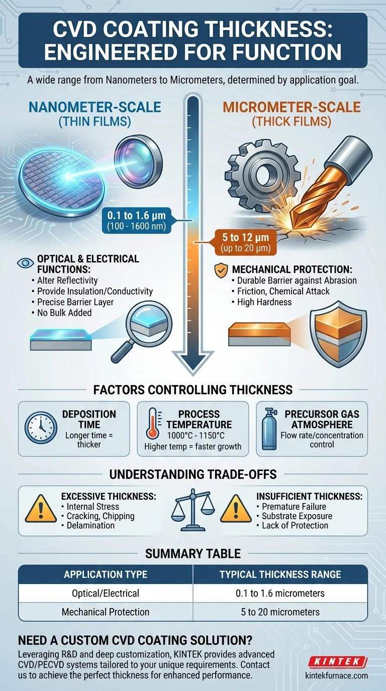
To be precise, the typical thickness for a Chemical Vapor Deposition (CVD) coating spans an exceptionally wide range, from hundreds of nanometers to over 10 micrometers. This is not a lack of process control, but a direct reflection of the coating's intended function. The required thickness is engineered based on whether the goal is to modify a surface's optical properties or to provide robust mechanical wear resistance.
The central takeaway is that there is no single "typical" thickness for a CVD coating. The thickness is a critical design parameter determined entirely by the application, generally falling into two distinct categories: thin films (nanometers) for optical/electrical functions and thick films (micrometers) for mechanical protection.
Why Such a Broad Range? Thickness as a Functional Parameter
The significant variation in CVD coating thickness stems from the diverse problems it is used to solve. The thickness is not a byproduct of the process; it is a primary input tailored to achieve a specific performance outcome.
Nanometer-Scale Coatings (Thin Films)
For applications in optics, semiconductors, and electronics, CVD coatings are incredibly thin, often in the 100 to 1600 nanometer (0.1 to 1.6 µm) range.
At this scale, the goal is not to add bulk but to create a new functional surface. These thin layers can alter light reflectivity, provide electrical insulation or conductivity, or act as a precise barrier layer without changing the part's dimensions.
Micrometer-Scale Coatings (Thick Films)
For heavy-duty industrial applications, such as coating cutting tools or wear-resistant components, much thicker layers are required. Here, the typical range is 5 to 12 micrometers (µm), and can extend up to 20 µm in special cases.
This substantial thickness is necessary to provide a durable barrier against abrasion, friction, and chemical attack. The coating's hardness and integrity depend on having enough material to withstand intense mechanical stress over its service life.
The Factors Controlling CVD Coating Thickness
Achieving a target thickness with high precision is a hallmark of the CVD process. This control is managed by manipulating several key process variables.
Deposition Time
The most direct factor is time. All other variables being equal, the longer a substrate is exposed to the precursor gases inside the reactor, the thicker the resulting coating will be.
Process Temperature
CVD is a high-temperature process, often running between 1000°C and 1150°C. Higher temperatures generally accelerate the chemical reactions that form the coating, leading to a faster deposition rate and a thicker film for a given amount of time.
Precursor Gas Atmosphere
The concentration and flow rate of the precursor gases (the chemical "building blocks") into the reaction chamber are meticulously controlled. A higher concentration of reactants can increase the growth rate, leading to a thicker coating.
Understanding the Trade-offs
Choosing a coating thickness is a balance between performance requirements and process limitations. Simply applying a thicker coating is not always better.
The Problem with Excessive Thickness
As a coating gets thicker, internal stresses can build up. If a coating is too thick for its intended material and geometry, it can become brittle, leading to cracking, chipping, or delamination from the substrate under thermal or mechanical stress.
The Limitation of Insufficient Thickness
Conversely, a coating that is too thin for a high-wear environment will fail prematurely. It will simply wear away, exposing the substrate and failing to provide the intended protection against abrasion or corrosion.
Process and Cost Constraints
Achieving very thick coatings (e.g., >20 µm) can be time-consuming and therefore expensive. Furthermore, prolonged exposure to the high temperatures of the CVD process can potentially affect the underlying properties of the substrate material itself.
Selecting the Right Thickness for Your Application
The optimal thickness is the thinnest possible layer that reliably meets your performance goal.
- If your primary focus is on optical or electrical properties: You will almost certainly require a thin-film coating measured in nanometers to achieve precise functional control without altering part dimensions.
- If your primary focus is on mechanical wear resistance: You will need a robust thick-film coating, typically measured in micrometers, to ensure durability and a long service life.
Ultimately, viewing coating thickness as a critical design specification is the key to leveraging the CVD process effectively.
Summary Table:
| Application Type | Typical Thickness Range | Key Functions |
|---|---|---|
| Optical/Electrical | 0.1 to 1.6 micrometers | Alters reflectivity, provides insulation/conductivity, acts as barrier |
| Mechanical Protection | 5 to 20 micrometers | Resists abrasion, friction, and chemical attack for durability |
Need a Custom CVD Coating Solution? Leveraging exceptional R&D and in-house manufacturing, KINTEK provides diverse laboratories with advanced high-temperature furnace solutions. Our product line, including Muffle, Tube, Rotary Furnaces, Vacuum & Atmosphere Furnaces, and CVD/PECVD Systems, is complemented by our strong deep customization capability to precisely meet unique experimental requirements. Whether you're working on optical, electrical, or mechanical applications, we can help you achieve the perfect coating thickness for enhanced performance and longevity. Contact us today to discuss your specific needs and discover how our tailored solutions can benefit your projects!
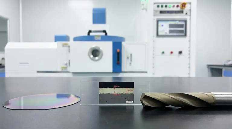
Visual Guide
Related Products
- HFCVD Machine System Equipment for Drawing Die Nano Diamond Coating
- Custom Made Versatile CVD Tube Furnace Chemical Vapor Deposition CVD Equipment Machine
- RF PECVD System Radio Frequency Plasma Enhanced Chemical Vapor Deposition
- Multi Heating Zones CVD Tube Furnace Machine for Chemical Vapor Deposition Equipment
- 915MHz MPCVD Diamond Machine Microwave Plasma Chemical Vapor Deposition System Reactor
People Also Ask
- How can customers maximize the quality of CVD coatings? Master Pre-Coating Prep for Superior Results
- What are the equipment for chemical vapor deposition? A Guide to the 5 Essential Components
- What core function does CVD equipment serve in h-BN anti-corrosion? Master Precision Synthesis for High-Performance Films
- What is the advantage of using a CVD system for coating turbine blades? Master Complex Geometries with Ease
- What is chemical vapor deposition (CVD) and its primary industrial application? Unlock Precision Thin Films for Electronics


