In solar cell production, Chemical Vapor Deposition (CVD) is a cornerstone manufacturing process used to create the essential thin-film layers that convert sunlight into electricity. It is not just one technique but a family of processes used to both build the core photovoltaic material and to add functional coatings that significantly boost the cell's overall efficiency and durability.
The core challenge in solar cell manufacturing is creating a perfectly structured, multi-layered semiconductor device at an industrial scale. CVD is significant because it provides the atomic-level precision required to deposit these ultra-thin films, directly determining the final performance and economic viability of the solar cell.
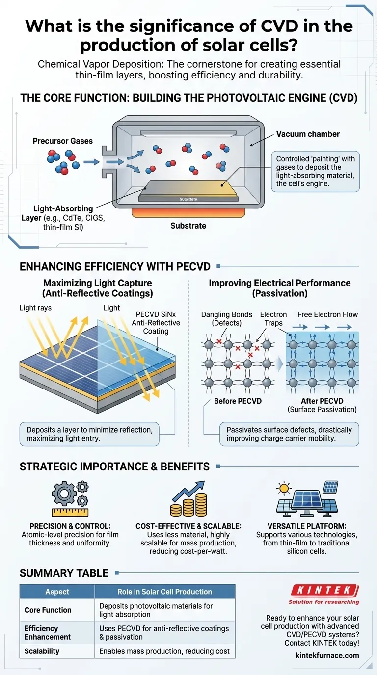
The Core Function: Building the Photovoltaic Engine
At its heart, a solar cell is a specialized semiconductor designed to capture photons and release electrons. CVD is the technology used to construct the most critical parts of this device.
What is Chemical Vapor Deposition?
Think of CVD as a highly controlled "painting" process using chemical gases. Precursor gases are introduced into a vacuum chamber containing the base material, or substrate. These gases react and decompose on the hot substrate surface, forming a solid, ultra-thin film with a highly ordered structure.
Depositing the Light-Absorbing Layer
The primary role of CVD is to deposit the photovoltaic material—the very layer that absorbs sunlight. This is the engine of the solar cell.
For thin-film solar cells, CVD is used to create layers of materials like cadmium telluride (CdTe), copper indium gallium selenide (CIGS), or various forms of thin-film silicon. The precise control CVD offers over the film's thickness and chemical composition is essential for optimizing the cell's light absorption and electrical properties.
Beyond the Engine: Enhancing Efficiency with PECVD
While standard CVD builds the core, a specialized, lower-temperature variant called Plasma-Enhanced CVD (PECVD) is critical for adding layers that enhance performance without damaging the underlying cell structure.
The Role of Plasma-Enhanced CVD (PECVD)
PECVD uses plasma to energize the precursor gases, allowing the deposition process to occur at much lower temperatures. This is vital when adding layers on top of already-fabricated parts of the solar cell that are sensitive to heat.
Maximizing Light Capture with Anti-Reflective Coatings
A significant portion of sunlight can reflect off the shiny surface of a solar cell, wasting potential energy. PECVD is used to deposit a transparent silicon nitride (SiNx) film that acts as an anti-reflective coating.
This layer is engineered to a specific thickness that minimizes reflection and maximizes the amount of light that enters the cell, directly increasing its power output.
Improving Electrical Performance Through Passivation
This is one of the most critical and subtle roles of PECVD. During manufacturing, microscopic defects, or "dangling bonds," can form on the surface of the silicon. These defects act as traps for the electrons freed by sunlight, reducing the cell's efficiency.
The hydrogen-rich silicon nitride film deposited by PECVD "passivates" these defects, effectively healing the surface. This surface passivation allows electrons to move more freely, drastically improving charge carrier mobility and the overall performance of the solar cell.
Understanding the Trade-offs and Strategic Importance
Like any advanced manufacturing process, CVD involves a balance of benefits and challenges that are crucial to understand.
Precision vs. Process Complexity
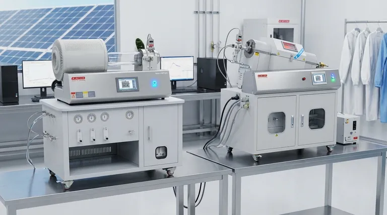
The greatest strength of CVD is its ability to control film thickness and uniformity with atomic-level precision. However, this requires sophisticated and expensive furnace systems that manage high vacuum, precise temperatures, and the controlled flow of reactive gases.
Cost-Effectiveness and Scalability
Thin-film solar cells, which rely heavily on CVD, use significantly less raw material than traditional thick silicon wafers. This, combined with the fact that CVD processes are highly scalable for mass production, is a key driver in reducing the overall cost-per-watt of solar energy.
A Versatile and Indispensable Tool
CVD's significance comes from its versatility. It is not limited to one type of solar technology. It is used to enhance traditional silicon wafer cells with passivation layers and is the foundational process for multiple generations of thin-film technologies, making it a vital platform for both current production and future innovation.
How to Apply This to Your Project
Your focus will determine which aspect of CVD technology is most relevant to your goals.
- If your primary focus is maximizing cell efficiency: The application of PECVD for depositing high-quality anti-reflective and passivation layers is your most critical area of interest.
- If your primary focus is developing next-generation, low-cost solar: Your attention should be on how CVD enables the deposition of novel thin-film materials like CdTe, CIGS, or perovskites.
- If your primary focus is industrial-scale manufacturing: The scalability, uniformity control, and throughput of large-area CVD systems are the most important factors for achieving economic viability.
Ultimately, CVD is the technology that transforms raw chemical gases into the high-performance heart of a modern solar cell, making it an indispensable enabler of clean energy.
Summary Table:
| Aspect | Role in Solar Cell Production |
|---|---|
| Core Function | Deposits photovoltaic materials (e.g., CdTe, CIGS) for light absorption |
| Efficiency Enhancement | Uses PECVD for anti-reflective coatings and surface passivation |
| Scalability | Enables mass production, reducing cost-per-watt |
| Versatility | Supports various solar technologies, including thin-film and silicon cells |
Ready to enhance your solar cell production with advanced high-temperature furnace solutions? KINTEK leverages exceptional R&D and in-house manufacturing to provide diverse laboratories with cutting-edge CVD/PECVD systems, Muffle Furnaces, Tube Furnaces, Rotary Furnaces, and Vacuum & Atmosphere Furnaces. Our strong deep customization capability ensures we meet your unique experimental needs for precise thin-film deposition, boosting efficiency and scalability. Contact us today to discuss how our solutions can drive your clean energy innovations forward!
Visual Guide
Related Products
- Cylindrical Resonator MPCVD Machine System for Lab Diamond Growth
- MPCVD Machine System Reactor Bell-jar Resonator for Lab and Diamond Growth
- HFCVD Machine System Equipment for Drawing Die Nano Diamond Coating
- RF PECVD System Radio Frequency Plasma Enhanced Chemical Vapor Deposition
- 915MHz MPCVD Diamond Machine Microwave Plasma Chemical Vapor Deposition System Reactor
People Also Ask
- How do carbon-containing groups contribute to diamond growth in the MPCVD method? Unlock High-Quality Diamond Synthesis
- What are the key components of an MPCVD system? Unlock High-Purity Crystal Growth
- What factors influence the quality of diamond deposition in the MPCVD method? Master the Critical Parameters for High-Quality Diamond Growth
- Why is temperature control important in the MPCVD growth process? Ensure High-Quality, Reliable Diamond Film Deposition
- How does MPCVD achieve stable temperature control during diamond growth? Master Precise Thermal Management


