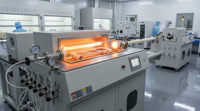
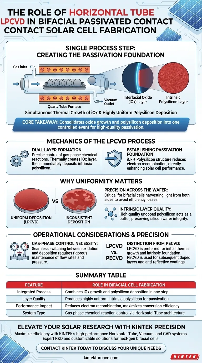
The Horizontal Tube Low Pressure Chemical Vapor Deposition (LPCVD) system serves as a critical manufacturing tool designed to deposit intrinsic polysilicon layers onto silicon wafers. Its primary role in this specific application is to execute a single process step that simultaneously achieves the thermal growth of an interfacial oxide (iOx) layer and the highly uniform deposition of polysilicon.
Core Takeaway The value of the Horizontal Tube LPCVD lies in its ability to consolidate two critical fabrication phases—oxide growth and polysilicon deposition—into one controlled event. This establishes the necessary foundation for high-quality passivation structures, which are essential for the efficiency of bifacial passivated contact solar cells.
The Mechanics of the LPCVD Process
Dual-Layer Formation
The system utilizes precise control over gas-phase chemical reactions to manage the wafer surface environment.
Rather than requiring separate equipment for oxidation and deposition, the Horizontal Tube LPCVD system creates the interfacial oxide (iOx) layer thermally. Immediately within the same sequence, it deposits the intrinsic polysilicon.
Establishing the Passivation Foundation
The combination of these two layers—the thin oxide and the polysilicon—forms the basis of the passivated contact.
This structure is vital for reducing electron recombination at the surface, which directly translates to higher solar cell performance. The LPCVD system ensures that this foundation is physically robust and chemically precise.
Why Uniformity Matters
Precision Across the Wafer
A key attribute of the Horizontal Tube LPCVD is its ability to deliver highly uniform deposition.
In bifacial cells, where light is harvested from both sides, inconsistencies in layer thickness can lead to significant efficiency losses. This system ensures the polysilicon layer is consistent across the entire wafer surface.
Intrinsic Layer Quality
While other methods (like PECVD) are often used for doped amorphous silicon or nitrides, the LPCVD system is specifically leveraged here for intrinsic (undoped) polysilicon.
This high-quality intrinsic layer acts as a buffer, preserving the integrity of the underlying silicon wafer before subsequent doping steps occur.
Operational Considerations and Precision
The Necessity of Gas-Phase Control
While the "single process step" offers efficiency, it introduces operational complexity. The system must switch between promoting thermal oxide growth and polysilicon deposition seamlessly.
This requires rigorous maintenance of gas flow rates and chamber pressure. Any deviation in the gas-phase reaction control can lead to poor oxide quality or uneven polysilicon coverage, compromising the cell's passivation capability.
Distinction from PECVD
It is important not to conflate this process with Plasma Enhanced CVD (PECVD).
While PECVD is standard for depositing doped amorphous layers or silicon nitride antireflective coatings later in the stack, the Horizontal Tube LPCVD is the preferred method for the initial, high-temperature thermal growth and intrinsic foundation required for passivated contacts.
Making the Right Choice for Your Goal
To maximize the effectiveness of your solar cell fabrication line, align your equipment choice with the specific layer requirements.
- If your primary focus is establishing the initial passivation structure: Prioritize the Horizontal Tube LPCVD for its ability to grow interfacial oxide and deposit intrinsic polysilicon in a single, uniform step.
- If your primary focus is depositing subsequent doped or anti-reflective layers: Utilize PECVD systems, which are better reflected in industry standards for handling amorphous silicon and silicon nitride layers.
Summary: The Horizontal Tube LPCVD is the definitive tool for creating the uniform, high-quality intrinsic foundation upon which high-efficiency bifacial passivated contacts are built.
Summary Table:
| Feature | Role in Bifacial Cell Fabrication |
|---|---|
| Integrated Process | Combines thermal oxide growth (iOx) and polysilicon deposition in one step |
| Layer Quality | Produces highly uniform intrinsic polysilicon layers essential for passivation |
| Performance Impact | Reduces electron recombination to maximize solar cell conversion efficiency |
| System Type | Gas-phase chemical reaction control via Horizontal Tube architecture |
Elevate Your Solar Research with KINTEK Precision
Maximize the efficiency of your solar cell fabrication with KINTEK’s high-performance laboratory solutions. Backed by expert R&D and world-class manufacturing, we provide high-temperature Horizontal Tube, Vacuum, and CVD systems specifically designed to meet the rigorous uniformity and gas-phase control requirements of passivated contact technology.
Whether you are developing next-generation bifacial cells or optimizing existing thin-film processes, our customizable systems offer the reliability and precision your lab demands. Ready to optimize your thin-film deposition?
Contact KINTEK Today to Discuss Your Unique Needs
Visual Guide
References
- Pradeep Padhamnath, Armin G. Aberle. Investigation of Contact Properties and Device Performance for Bifacial Double-Side Textured Silicon Solar Cells With Polysilicon Based Passivating Contacts. DOI: 10.52825/siliconpv.v2i.1295
This article is also based on technical information from Kintek Furnace Knowledge Base .
Related Products
- Custom Made Versatile CVD Tube Furnace Chemical Vapor Deposition CVD Equipment Machine
- Slide PECVD Tube Furnace with Liquid Gasifier PECVD Machine
- HFCVD Machine System Equipment for Drawing Die Nano Diamond Coating
- RF PECVD System Radio Frequency Plasma Enhanced Chemical Vapor Deposition
- Multi Heating Zones CVD Tube Furnace Machine for Chemical Vapor Deposition Equipment
People Also Ask
- What are the practical applications of gate media prepared by CVD tube furnaces? Unlock Advanced Electronics and More
- What is a CVD tube furnace and what is its primary function? Discover Precision Thin-Film Deposition
- What customization options are available for CVD tube furnaces? Tailor Your System for Superior Material Synthesis
- How can integrating CVD tube furnaces with other technologies benefit device fabrication? Unlock Advanced Hybrid Processes
- Which industries and research fields benefit from CVD tube furnace sintering systems for 2D materials? Unlock Next-Gen Tech Innovations


