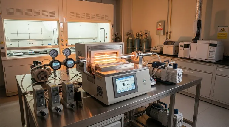
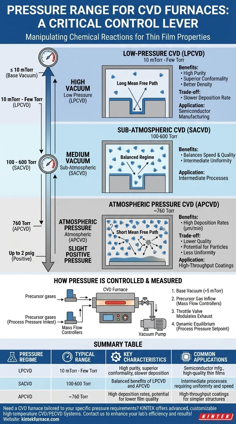
At its core, a Chemical Vapor Deposition (CVD) furnace operates across a pressure spectrum that extends from high vacuum to slightly above atmospheric pressure. Most commercial and research systems are designed to be controlled precisely anywhere from a few millitorr (mTorr) up to 760 Torr (standard atmospheric pressure), with some capable of handling slightly positive pressures up to 2 psig.
The specific pressure range of a CVD furnace is not just a technical specification; it is the primary control lever for manipulating the chemical reactions at the heart of the process. Understanding whether to use a high- or low-pressure regime is fundamental to controlling the final properties, quality, and deposition speed of the thin film.
The Role of Pressure in a CVD Process
Pressure inside the reaction chamber directly influences the concentration and behavior of the precursor gas molecules. It is one of the three critical pillars of CVD control, alongside temperature and gas flow rate.
Defining the Operating Regimes
CVD processes are often categorized by their operating pressure, as this fundamentally changes the deposition dynamics.
- Low-Pressure CVD (LPCVD): This regime typically operates from approximately 10 mTorr to a few Torr. The reduced pressure increases the mean free path—the average distance a gas molecule travels before colliding with another.
- Atmospheric Pressure CVD (APCVD): As the name implies, this process occurs at or near standard atmospheric pressure (760 Torr). The mean free path of molecules is extremely short, leading to very different reaction conditions.
- Sub-Atmospheric CVD (SACVD): This is a middle ground, operating between the LPCVD and APCVD ranges (roughly 100-600 Torr). It aims to balance the benefits of both regimes.
How Pressure Dictates Film Properties
The pressure setting directly impacts the final material. Lowering the pressure reduces the concentration of precursor gas, which slows the rate of chemical reactions both on the substrate and in the gas phase.
This leads to a process that is more dependent on surface reactions, resulting in films with higher purity, better density, and superior conformality—the ability to uniformly coat complex, non-flat surfaces.
How Pressure is Controlled and Measured
Achieving and maintaining a precise pressure is a multi-step process managed by an integrated control system. This is not a static setting but a dynamic equilibrium.
The Role of Vacuum Pumps
First, a mechanical pump or a series of pumps creates a base vacuum within the furnace chamber. This removes atmospheric gases and contaminants. A typical base vacuum might be below 5 mTorr, creating a clean environment before the process begins.
From Base Vacuum to Process Pressure
Once the base vacuum is achieved, precursor gases are introduced into the chamber through mass flow controllers. Simultaneously, a throttle valve located between the chamber and the vacuum pump modulates the exhaust rate.
The control system balances the inflow of gas with the outflow through the throttle valve to maintain a stable and precise process pressure at the desired setpoint, whether it's 500 mTorr for an LPCVD process or 760 Torr for APCVD.
Understanding the Trade-offs
The choice between a high-pressure and low-pressure process is a critical decision driven by the specific goals of the deposition. There is no single "best" pressure; there is only the right pressure for the application.
High Pressure (APCVD): Speed vs. Quality
Operating at atmospheric pressure provides a very high concentration of precursor molecules near the substrate. This results in very high deposition rates, often measured in micrometers per minute.
The primary trade-off is control. The short mean free path can lead to unwanted reactions in the gas phase, which can create particles that fall onto the film, reducing its quality. Uniformity can also be a challenge.
Low Pressure (LPCVD): Conformality vs. Speed
Operating under vacuum significantly reduces the deposition rate because there are fewer precursor molecules available to react.
The key benefit is exceptional film quality. The long mean free path of molecules allows them to reach and coat intricate topographies uniformly, making LPCVD the standard for applications requiring high-purity and highly conformal films, such as in semiconductor manufacturing.
Making the Right Choice for Your Application
Selecting the correct pressure regime is essential for achieving your desired material outcomes efficiently and cost-effectively.
- If your primary focus is high throughput for simpler coatings: APCVD is often the superior choice due to its rapid deposition speed.
- If your primary focus is high-purity, uniform films on complex 3D structures: LPCVD is the necessary and standard approach.
- If you are in a research & development environment: A flexible system capable of operating across the entire spectrum from mTorr to atmospheric pressure provides the greatest capability for material discovery.
Ultimately, pressure is the dial you turn to engineer the very environment in which your material is created.
Summary Table:
| Pressure Regime | Typical Range | Key Characteristics | Common Applications |
|---|---|---|---|
| Low-Pressure CVD (LPCVD) | 10 mTorr to a few Torr | High purity, superior conformality, slower deposition | Semiconductor manufacturing, high-quality thin films |
| Sub-Atmospheric CVD (SACVD) | 100-600 Torr | Balanced benefits of LPCVD and APCVD | Intermediate processes requiring uniformity and speed |
| Atmospheric Pressure CVD (APCVD) | ~760 Torr | High deposition rates, potential for lower film quality | High-throughput coatings for simpler structures |
Need a CVD furnace tailored to your specific pressure requirements? At KINTEK, we leverage exceptional R&D and in-house manufacturing to provide advanced high-temperature furnace solutions, including CVD/PECVD Systems. Our strong deep customization capability ensures we precisely meet your unique experimental needs for optimal thin film deposition. Contact us today to discuss how we can enhance your lab's efficiency and results!
Visual Guide
Related Products
- Custom Made Versatile CVD Tube Furnace Chemical Vapor Deposition CVD Equipment Machine
- Split Chamber CVD Tube Furnace with Vacuum Station CVD Machine
- Multi Heating Zones CVD Tube Furnace Machine for Chemical Vapor Deposition Equipment
- Slide PECVD Tube Furnace with Liquid Gasifier PECVD Machine
- Controlled Inert Nitrogen Hydrogen Atmosphere Furnace
People Also Ask
- What customization options are available for CVD tube furnaces? Tailor Your System for Superior Material Synthesis
- What are the practical applications of gate media prepared by CVD tube furnaces? Unlock Advanced Electronics and More
- Which industries and research fields benefit from CVD tube furnace sintering systems for 2D materials? Unlock Next-Gen Tech Innovations
- Why are CVD tube furnace sintering systems indispensable for 2D material research and production? Unlock Atomic-Scale Precision
- How might AI and machine learning enhance CVD tube furnace processes? Boost Quality, Speed, and Safety


