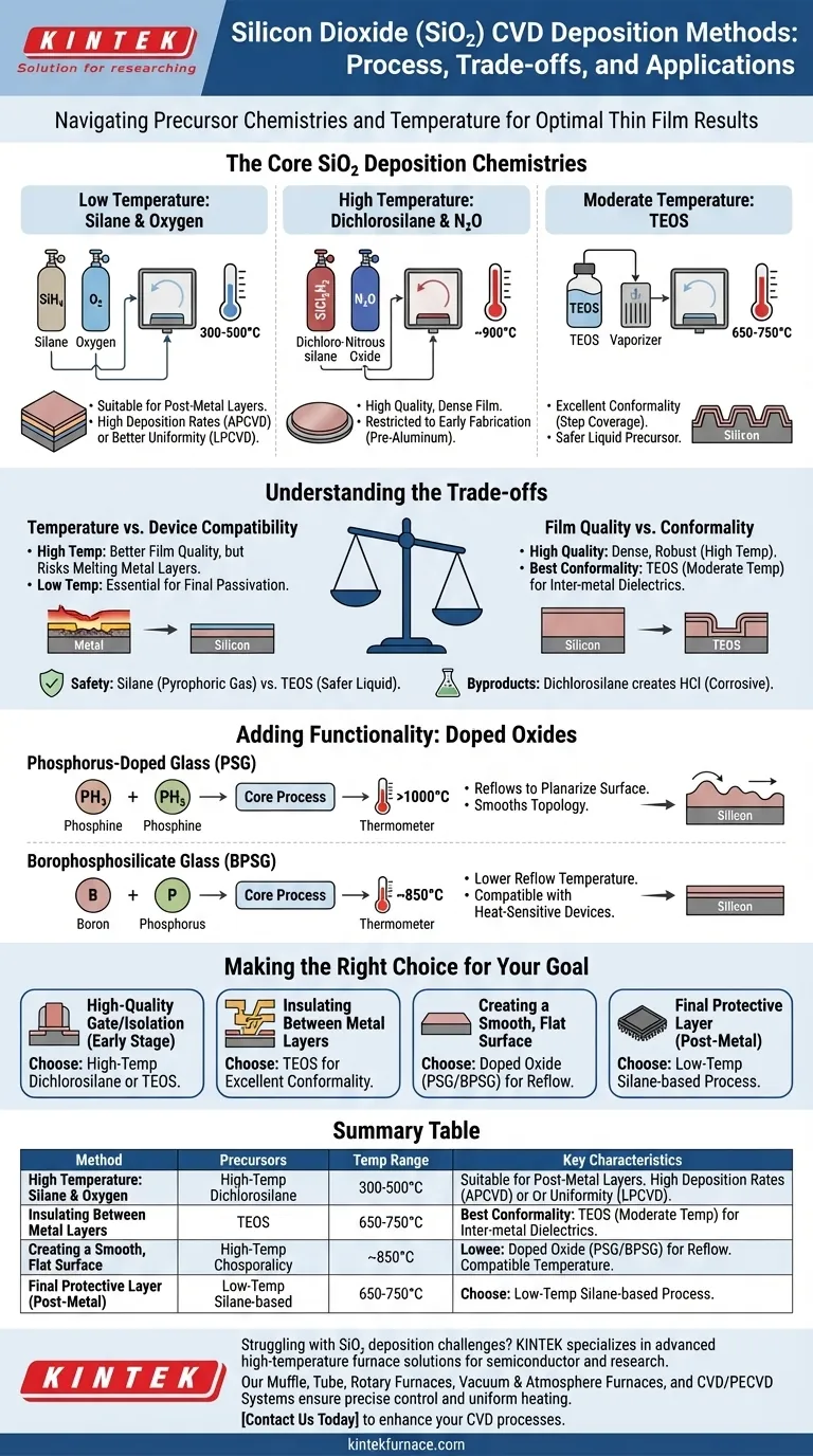
In short, the primary methods for depositing silicon dioxide (SiO₂) via Chemical Vapor Deposition (CVD) involve reacting specific precursor gases at different temperatures. The three most common chemistries are the reaction of silane with oxygen at low temperatures (300-500°C), the reaction of dichlorosilane with nitrous oxide at high temperatures (~900°C), and the thermal decomposition of tetraethylorthosilicate (TEOS) at moderate temperatures (650-750°C).
Choosing a method for SiO₂ deposition is not about finding the "best" one, but about making a strategic trade-off. The decision hinges on the required deposition temperature, the geometric complexity of the device, and the desired quality of the resulting film.
The Core SiO₂ Deposition Chemistries
Each chemical pathway for creating SiO₂ offers a distinct set of characteristics. The choice is determined by the specific requirements of the manufacturing step.
Silane and Oxygen (Low Temperature)
This process reacts silane gas (SiH₄) with oxygen (O₂) at relatively low temperatures, typically between 300°C and 500°C.
It is often performed in Atmospheric Pressure CVD (APCVD) systems for high deposition rates, or Low-Pressure CVD (LPCVD) for better uniformity. Its low-temperature nature makes it suitable for deposition steps that occur after temperature-sensitive metal layers have already been fabricated.
Dichlorosilane and Nitrous Oxide (High Temperature)
This method uses dichlorosilane (SiCl₂H₂) and nitrous oxide (N₂O) at approximately 900°C.
The high temperature results in a very high-quality, dense silicon dioxide film. However, this temperature restricts its use to early stages of fabrication, before aluminum or other low-melting-point metals are present on the device.
Tetraethylorthosilicate (TEOS)
This process involves the thermal decomposition of a liquid precursor, tetraethylorthosilicate (TEOS), at temperatures between 650°C and 750°C.
TEOS is renowned for producing films with excellent conformality, meaning it can uniformly coat complex, non-flat surfaces with sharp steps. This, combined with its safer liquid form compared to pyrophoric silane gas, makes it a workhorse in modern semiconductor manufacturing.
Understanding the Trade-offs
Selecting the right process requires balancing competing factors. What you gain in one area, you often sacrifice in another.
Temperature vs. Device Compatibility
This is the most critical trade-off. High-temperature processes like the dichlorosilane method yield excellent films but can damage or melt previously deposited metal layers.
Low-temperature processes using silane are essential for layers deposited late in the manufacturing flow, such as the final protective passivation layer over the metal bond pads.
Film Quality and Conformality
High-quality films are dense, uniform, and electrically robust. Generally, higher deposition temperatures produce higher-quality films.
However, conformality, or step coverage, is equally critical for insulating the microscopic vertical features of a modern chip. TEOS-based processes offer the best conformality, making them indispensable for inter-metal dielectrics.
Safety and Byproducts
Precursor choice has significant safety implications. Silane (SiH₄) is a pyrophoric gas that ignites on contact with air, requiring strict handling protocols. TEOS is a liquid, which is far safer to store and handle.
Additionally, some reactions produce corrosive byproducts. The dichlorosilane process, for instance, creates hydrochloric acid (HCl), which must be managed to prevent damage to the equipment and the wafer.
Adding Functionality: Doped Oxides
Sometimes, pure silicon dioxide is not enough. Impurities can be intentionally added during deposition to change the film's properties. This is known as doping.
Phosphorus-Doped Glass (PSG)
By adding phosphine gas (PH₃) to the CVD process, you create phosphorus-doped glass, or PSG.
The key benefit of PSG is that it "reflows," or softens and smooths out, at temperatures above 1000°C. This is used to planarize the surface, creating a flatter topology for subsequent layers.
Borophosphosilicate Glass (BPSG)
By adding both boron and phosphorus precursors, you create borophosphosilicate glass, or BPSG.
BPSG's primary advantage is its lower reflow temperature of around 850°C. This ability to planarize a surface at a lower temperature makes it more compatible with devices that cannot tolerate the high heat required to reflow standard PSG.
Making the Right Choice for Your Goal
Your application dictates the optimal SiO₂ deposition strategy.
- If your primary focus is a high-quality gate or isolation oxide early in the process: A high-temperature dichlorosilane or TEOS process is the ideal choice.
- If your primary focus is insulating between metal layers: A TEOS-based process is preferred for its excellent conformality and moderate temperature.
- If your primary focus is creating a smooth, flat surface for subsequent layers: Use a doped oxide like PSG or BPSG to leverage their thermal reflow properties.
- If your primary focus is a final protective layer over the finished device: A low-temperature silane-based process is necessary to avoid damaging the underlying metal circuitry.
Ultimately, mastering SiO₂ deposition is about understanding your constraints and selecting the chemical process that best aligns with your specific technical objective.
Summary Table:
| Method | Precursors | Temperature Range | Key Characteristics |
|---|---|---|---|
| Silane and Oxygen | SiH₄, O₂ | 300-500°C | Low temperature, suitable for post-metal layers |
| Dichlorosilane and Nitrous Oxide | SiCl₂H₂, N₂O | ~900°C | High quality, dense film, early fabrication stages |
| TEOS | TEOS | 650-750°C | Excellent conformality, safer liquid precursor |
Struggling with SiO₂ deposition challenges in your lab? KINTEK specializes in advanced high-temperature furnace solutions tailored for semiconductor and materials research. Our Muffle, Tube, Rotary Furnaces, Vacuum & Atmosphere Furnaces, and CVD/PECVD Systems, backed by deep customization, ensure precise temperature control and uniform heating for optimal film quality. Whether you need low-temperature processes for sensitive devices or high-conformality coatings, we deliver reliable, efficient solutions. Contact us today to discuss how KINTEK can enhance your CVD processes and accelerate your innovations!
Visual Guide
Related Products
- Custom Made Versatile CVD Tube Furnace Chemical Vapor Deposition CVD Equipment Machine
- Multi Heating Zones CVD Tube Furnace Machine for Chemical Vapor Deposition Equipment
- Slide PECVD Tube Furnace with Liquid Gasifier PECVD Machine
- Inclined Rotary Plasma Enhanced Chemical Deposition PECVD Tube Furnace Machine
- Cylindrical Resonator MPCVD Machine System for Lab Diamond Growth
People Also Ask
- What customization options are available for CVD tube furnaces? Tailor Your System for Superior Material Synthesis
- What are the benefits of developing new precursor materials for CVD tube furnaces? Unlock Advanced Thin-Film Synthesis
- What are the practical applications of gate media prepared by CVD tube furnaces? Unlock Advanced Electronics and More
- Why are CVD tube furnace sintering systems indispensable for 2D material research and production? Unlock Atomic-Scale Precision
- How does CVD tube furnace sintering enhance graphene growth? Achieve Superior Crystallinity and High Electron Mobility


