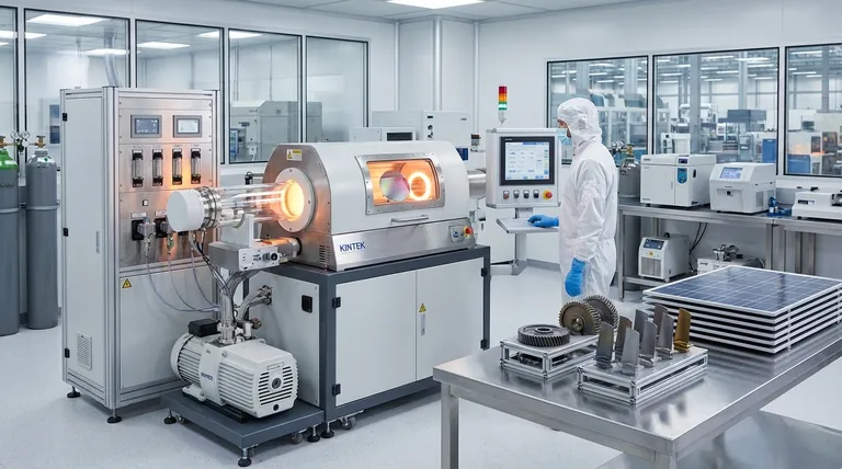
At its core, Chemical Vapor Deposition (CVD) is a foundational manufacturing process used to create high-performance, ultra-thin films on a material's surface. Its applications are vast, spanning industries from semiconductor manufacturing, where it's used to build integrated circuits and solar panels, to the aerospace and automotive sectors, where it creates protective coatings that resist corrosion and wear.
The true value of CVD lies not in a single process, but in its versatility as a family of techniques. By precisely controlling the deposition of atoms and molecules, CVD allows engineers to fundamentally change a material's surface properties—making it more durable, electrically conductive, or chemically resistant to solve specific industrial challenges.
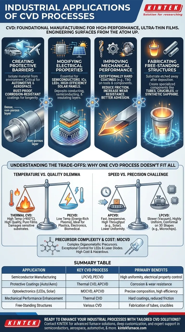
The Core Function: Engineering Surfaces from the Atom Up
CVD is not merely a coating process; it is a method of building new material layers with atomic precision. This capability is applied to achieve several distinct industrial outcomes.
Creating Protective Barriers
The most common application of CVD is to deposit a thin, dense, and non-porous film that isolates the underlying material from its environment.
This is critical in the automotive and aerospace industries for creating rust-proof and corrosion-resistant coatings on metal parts, dramatically enhancing material longevity and reliability.
Modifying Electrical Properties
The semiconductor industry is arguably the largest user of CVD. The process is essential for depositing the multiple layers of conducting, semiconducting, and insulating materials that form an integrated circuit (IC).
Without CVD, the mass production of microchips, LEDs, and high-efficiency solar panels would be impossible. It provides the control needed to build the complex, layered structures that define modern electronics.
Improving Mechanical Performance
CVD is used to create exceptionally hard coatings on tools, bearings, and engine components. These coatings, often composed of materials like titanium nitride, drastically reduce friction and increase resistance to wear.
It is also used for surface modification to promote better adhesion between different layers of a material, ensuring components remain bonded under stress.
Fabricating Free-Standing Structures
In advanced applications, the original material (substrate) can be chemically etched away after deposition.
This leaves behind a free-standing, thin but solid structure made entirely of the CVD-deposited material. This technique is used to create specialized components like tubes, crucibles, or single-crystal materials like synthetic sapphire.
Understanding the Trade-offs: Why One CVD Process Doesn't Fit All
The term "CVD" describes a wide range of processes, each with its own advantages and limitations. The choice of technique is dictated by the material being coated, the desired properties of the film, and economic factors.
The Temperature vs. Quality Dilemma
Traditional Thermal CVD relies on high temperatures (often >900°C) to drive chemical reactions, typically producing very high-quality, pure films. However, these temperatures can damage or destroy sensitive substrates like plastics or complex electronic components.
Plasma-Enhanced CVD (PECVD) solves this by using an energy-rich plasma to initiate the reaction. This allows deposition to occur at much lower temperatures, making it ideal for modern electronics, biomedical devices, and flexible substrates.
The Speed vs. Precision Challenge
Atmospheric Pressure CVD (APCVD) is fast and relatively inexpensive, making it suitable for high-throughput applications like coating solar cells. Its downside is often a lower degree of film uniformity.
Conversely, Low-Pressure CVD (LPCVD) operates in a vacuum. While slower, it produces highly uniform and conformal coatings that can cover complex, 3D shapes, making it a workhorse for manufacturing high-density microchips.
Precursor Complexity and Cost
Metal-Organic CVD (MOCVD) uses complex organometallic compounds as precursors. This process offers exceptional control over the composition and crystalline structure of the film, which is essential for manufacturing high-performance LEDs and laser diodes.
The trade-off is the high cost and hazardous nature of the precursor materials, which requires sophisticated handling and safety systems.
Making the Right Choice for Your Goal
Selecting the appropriate CVD method requires aligning the process capabilities with the specific requirements of the end product.
- If your primary focus is mass production of robust components like solar cells or basic coatings: APCVD offers the speed and cost-effectiveness needed for large-scale manufacturing.
- If your primary focus is creating highly uniform films for microelectronics: LPCVD is the industry standard for its ability to produce high-quality, conformal layers essential for integrated circuits.
- If your primary focus is coating temperature-sensitive materials like plastics or advanced sensors: PECVD is the necessary choice to avoid damaging the underlying substrate.
- If your primary focus is fabricating advanced optoelectronics like high-brightness LEDs: MOCVD provides the unmatched compositional control required for these complex crystalline structures.
Understanding this direct link between the industrial application and the specific CVD technique is the key to harnessing its full manufacturing potential.
Summary Table:
| Application | Key CVD Process | Primary Benefits |
|---|---|---|
| Semiconductor Manufacturing | LPCVD, PECVD | High uniformity, electrical property control |
| Protective Coatings (e.g., automotive, aerospace) | Thermal CVD, APCVD | Corrosion and wear resistance |
| Optoelectronics (e.g., LEDs, solar panels) | MOCVD, APCVD | Precise composition, high efficiency |
| Mechanical Performance Enhancement | Thermal CVD | Hard coatings, reduced friction |
| Free-Standing Structures | Various CVD | Fabrication of tubes, crucibles |
Ready to enhance your industrial processes with tailored CVD solutions? At KINTEK, we leverage exceptional R&D and in-house manufacturing to provide advanced high-temperature furnace solutions, including CVD/PECVD Systems, Muffle, Tube, Rotary Furnaces, and Vacuum & Atmosphere Furnaces. Our strong deep customization capability ensures we precisely meet your unique experimental and production requirements, whether you're in semiconductors, aerospace, automotive, or other sectors. Contact us today to discuss how our expertise can drive innovation and efficiency in your projects!
Visual Guide
Related Products
- Custom Made Versatile CVD Tube Furnace Chemical Vapor Deposition CVD Equipment Machine
- Split Chamber CVD Tube Furnace with Vacuum Station CVD Machine
- Multi Heating Zones CVD Tube Furnace Machine for Chemical Vapor Deposition Equipment
- Slide PECVD Tube Furnace with Liquid Gasifier PECVD Machine
- Controlled Inert Nitrogen Hydrogen Atmosphere Furnace
People Also Ask
- How does CVD tube furnace sintering enhance graphene growth? Achieve Superior Crystallinity and High Electron Mobility
- What customization options are available for CVD tube furnaces? Tailor Your System for Superior Material Synthesis
- Which industries and research fields benefit from CVD tube furnace sintering systems for 2D materials? Unlock Next-Gen Tech Innovations
- What improvements can be made to the bonding force of gate dielectric films using a CVD tube furnace? Enhance Adhesion for Reliable Devices
- How might AI and machine learning enhance CVD tube furnace processes? Boost Quality, Speed, and Safety


