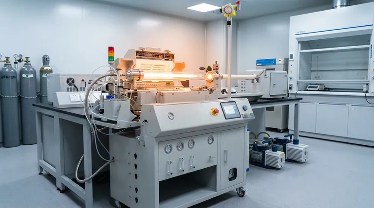
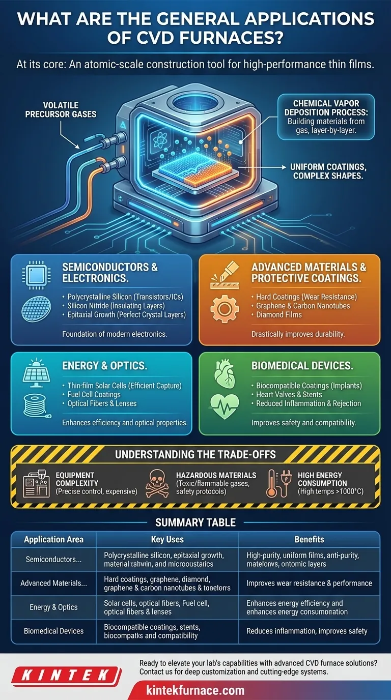
At its core, a Chemical Vapor Deposition (CVD) furnace is used for a vast range of applications centered on creating high-purity, high-performance thin films and engineered coatings. This technology is foundational to numerous high-tech industries, including semiconductor manufacturing, advanced materials science, energy, and the biomedical field. It enables the precise deposition of materials onto a substrate to enhance or fundamentally change its properties.
The true purpose of a CVD furnace is not simply to heat a sample, but to facilitate a chemical reaction on a molecular level. It is an atomic-scale construction tool, allowing engineers and scientists to build custom material layers from a gaseous state, unlocking properties that are otherwise unattainable.
The Core Principle: Building Materials from Gas
What is Chemical Vapor Deposition?
Chemical Vapor Deposition is a process where a substrate (the object to be coated) is placed inside the furnace chamber under controlled temperature and pressure.
Volatile precursor gases are then introduced into the chamber. These gases react or decompose on and near the hot substrate surface, leaving behind a solid material in the form of a thin film.
Why This Method is Powerful
This layer-by-layer deposition allows for incredible control over the film's purity, thickness, and structure. Because the process starts from a gas, it can create uniform coatings on substrates with highly complex shapes, a feat difficult for many other coating methods.
Key Applications Across Industries
The ability to engineer surfaces at the atomic level gives CVD furnaces an incredibly broad range of applications.
Semiconductors and Electronics
This is arguably the most significant application of CVD. The entire modern electronics industry relies on the thin films created in these furnaces.
Uses include depositing the ultra-pure polycrystalline silicon that forms the basis of transistors, diodes, and integrated circuits. It is also used for depositing insulating layers like silicon nitride and for the epitaxial growth of perfect crystal layers on silicon wafers.
Advanced Materials and Protective Coatings
CVD is used to create some of the most durable and advanced materials known. This involves depositing a hard, functional layer onto a base material to drastically improve its performance.
Common examples include hard coatings on cutting tools and turbine blades to improve wear resistance and lifespan. The process is also used to synthesize advanced materials like graphene, carbon nanotubes, and diamond films.
Energy and Optics
In the energy sector, CVD is critical for manufacturing thin-film solar cells, where different material layers are deposited to efficiently capture and convert sunlight. It is also used to apply protective and functional coatings to fuel cell components.
For optics, the process creates specialized films on lenses and mirrors and is integral to the fabrication of optical fibers by depositing materials with specific refractive properties.
Biomedical Devices
CVD allows for the creation of biocompatible coatings that improve the safety and performance of medical implants.
A key application is coating devices like heart valves and vascular stents with inert, wear-resistant materials. These coatings enhance compatibility with biological tissue, reducing the risk of inflammation and rejection by the body.
Understanding the Trade-offs
While powerful, the CVD process involves significant complexity and investment. It is not a universally simple or low-cost solution.
Equipment and Process Complexity
Achieving the required high-purity films demands precise control over temperature, pressure, and gas flow rates. This necessitates sophisticated, and often expensive, furnace systems with advanced vacuum and gas handling capabilities.
Hazardous Materials
The precursor gases used in many CVD processes can be toxic, flammable, or corrosive. This requires strict safety protocols, specialized storage, and exhaust gas treatment systems, adding to the operational overhead.
High Energy Consumption
CVD furnaces often operate at very high temperatures, sometimes exceeding 1000°C. This leads to significant energy consumption, which is a primary cost driver for high-volume manufacturing.
Making the Right Choice for Your Goal
To apply this technology effectively, you must align its capabilities with your primary objective.
- If your primary focus is mass-producing electronic components: CVD is the non-negotiable industry standard for creating the foundational silicon and dielectric films in semiconductor fabrication.
- If your primary focus is enhancing the durability of a product: CVD is an elite method for applying ultra-hard, wear-resistant, or corrosion-proof coatings to tools, engine parts, and other high-performance components.
- If your primary focus is developing next-generation technology: CVD provides a flexible platform for research and development, enabling the synthesis of advanced materials and novel surfaces for fields like nanotechnology, catalysis, and biomedicine.
Ultimately, the CVD furnace is a cornerstone technology that transforms passive surfaces into active, high-performance components.
Summary Table:
| Application Area | Key Uses | Benefits |
|---|---|---|
| Semiconductors and Electronics | Deposition of polycrystalline silicon, silicon nitride, epitaxial growth | Enables high-purity, uniform films for reliable electronic components |
| Advanced Materials and Protective Coatings | Hard coatings on tools, synthesis of graphene, carbon nanotubes, diamond films | Improves wear resistance, durability, and material performance |
| Energy and Optics | Thin-film solar cells, fuel cell coatings, optical fibers, lenses | Enhances energy efficiency and optical properties |
| Biomedical Devices | Biocompatible coatings on heart valves, stents | Reduces inflammation, improves implant safety and compatibility |
Ready to elevate your lab's capabilities with advanced CVD furnace solutions? At KINTEK, we leverage exceptional R&D and in-house manufacturing to provide diverse laboratories with cutting-edge high-temperature furnace systems. Our product line includes CVD/PECVD Systems, Muffle, Tube, Rotary Furnaces, and Vacuum & Atmosphere Furnaces, all backed by strong deep customization to precisely meet your unique experimental needs. Whether you're in semiconductor production, materials science, energy, or biomedical research, we can help you achieve superior thin-film deposition and performance enhancements. Contact us today to discuss how our tailored solutions can drive your innovations forward!
Visual Guide
Related Products
- Custom Made Versatile CVD Tube Furnace Chemical Vapor Deposition CVD Equipment Machine
- Split Chamber CVD Tube Furnace with Vacuum Station CVD Machine
- Multi Heating Zones CVD Tube Furnace Machine for Chemical Vapor Deposition Equipment
- Slide PECVD Tube Furnace with Liquid Gasifier PECVD Machine
- Inclined Rotary Plasma Enhanced Chemical Deposition PECVD Tube Furnace Machine
People Also Ask
- What are the practical applications of gate media prepared by CVD tube furnaces? Unlock Advanced Electronics and More
- How does CVD tube furnace sintering enhance graphene growth? Achieve Superior Crystallinity and High Electron Mobility
- What temperature range do standard CVD tube furnaces operate at? Unlock Precision for Your Material Deposition
- What are the key features of CVD tube furnaces for 2D material processing? Unlock Precision Synthesis for Superior Materials
- Which industries and research fields benefit from CVD tube furnace sintering systems for 2D materials? Unlock Next-Gen Tech Innovations


