At its core, the primary benefit of an enhanced growth rate in a Chemical Vapor Deposition (CVD) furnace is a significant increase in manufacturing throughput. By accelerating the material deposition process, these systems enable faster production cycles, allowing manufacturers to produce more components in less time and meet demanding market schedules.
The central challenge is not merely achieving speed, but achieving it without sacrificing material quality. Enhanced growth rates are only valuable when paired with advanced control systems that can maintain film uniformity and minimize defects, transforming speed from a liability into a powerful economic advantage.
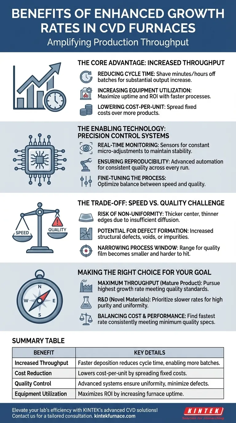
The Core Advantage: Amplifying Production Throughput
A higher growth rate directly translates to improved operational efficiency and a stronger bottom line. This is the primary driver for investing in and optimizing high-speed CVD processes.
Reducing Cycle Time
The most direct benefit is a reduction in the time required to deposit a film of a specific thickness. For high-volume manufacturing, shaving minutes or hours off each batch adds up to a substantial increase in overall output.
Increasing Equipment Utilization
Expensive CVD furnaces are a major capital investment. A faster process means a single furnace can run more batches per day, maximizing its uptime and delivering a faster return on investment (ROI).
Lowering Cost-Per-Unit
By producing more units in the same amount of time, the fixed costs of operation—such as energy, facility overhead, and labor—are spread across a larger number of products. This systematically drives down the manufacturing cost of each individual component.
The Enabling Technology: Precision Control Systems
High growth rates are not achieved by simply turning up the heat or gas flow. They are made possible by sophisticated control systems that manage the inherent volatility of a rapid deposition process.
Real-Time Monitoring and Adjustment
Modern CVD furnaces use sensors to provide real-time feedback on critical parameters like temperature, pressure, and gas concentration. The control system uses this data to make constant micro-adjustments, ensuring the process remains stable within a very tight window.
Ensuring Reproducibility
At high speeds, small deviations can quickly lead to failed batches. Advanced automation and programmable process recipes ensure that every run is executed with identical parameters, guaranteeing reproducibility and consistent quality from the first unit to the thousandth.
Fine-Tuning the Process
These control systems give engineers the ability to fine-tune dozens of variables to find the optimal balance between speed and quality for a specific material. This level of control is essential for developing and scaling a robust, high-yield manufacturing process.
Understanding the Trade-offs: The Challenge of Speed vs. Quality
While the references state that speed can be achieved "without compromising quality," this represents an ideal outcome, not a guaranteed one. In practice, pushing for higher growth rates introduces significant material science challenges.
Risk of Non-Uniformity
At very high deposition rates, the precursor gases may not have sufficient time to diffuse evenly across the entire surface of the substrate. This can result in a film that is thicker in the center and thinner at the edges, failing to meet specifications.
Potential for Defect Formation
A faster process can be more chaotic at the atomic level. This can increase the likelihood of creating structural defects, voids, or unwanted impurities within the material, which can severely degrade its electrical, optical, or mechanical properties.
The "Process Window" Narrows
The "process window" is the range of temperature, pressure, and flow rates that produces a high-quality film. As you increase the growth rate, this window becomes significantly smaller and harder to hit. This is why high-speed systems are so reliant on the advanced, real-time control systems mentioned earlier.
Making the Right Choice for Your Goal
The ideal growth rate is not a universal number; it depends entirely on your specific objective.
- If your primary focus is maximum throughput for a mature product: Pursue the highest growth rate your system can achieve while still meeting quality control standards, as this will maximize profitability.
- If your primary focus is research and development of novel materials: Prioritize slower growth rates to achieve the highest possible film purity and uniformity, allowing for accurate characterization of the material's fundamental properties.
- If your primary focus is balancing cost and performance: Methodically test to find the fastest possible growth rate that consistently meets your product's minimum quality specifications, optimizing for the lowest cost-per-unit that satisfies the application.
Ultimately, mastering the CVD process is about controlling the delicate balance between manufacturing speed and atomic-level quality.
Summary Table:
| Benefit | Key Details |
|---|---|
| Increased Throughput | Faster deposition reduces cycle time, enabling more batches per day. |
| Cost Reduction | Lowers cost-per-unit by spreading fixed costs over more products. |
| Quality Control | Advanced systems ensure film uniformity and minimize defects at high speeds. |
| Equipment Utilization | Maximizes ROI by increasing furnace uptime and batch frequency. |
Elevate your lab's efficiency with KINTEK's advanced CVD solutions! Leveraging exceptional R&D and in-house manufacturing, we provide diverse laboratories with high-temperature furnace systems like CVD/PECVD, Muffle, Tube, Rotary, Vacuum, and Atmosphere Furnaces. Our strong deep customization capability ensures precise alignment with your unique experimental needs, boosting throughput and reducing costs. Ready to optimize your process? Contact us today for a tailored consultation!
Visual Guide
Related Products
- Custom Made Versatile CVD Tube Furnace Chemical Vapor Deposition CVD Equipment Machine
- Split Chamber CVD Tube Furnace with Vacuum Station CVD Machine
- Multi Heating Zones CVD Tube Furnace Machine for Chemical Vapor Deposition Equipment
- Slide PECVD Tube Furnace with Liquid Gasifier PECVD Machine
- Controlled Inert Nitrogen Hydrogen Atmosphere Furnace
People Also Ask
- How might AI and machine learning enhance CVD tube furnace processes? Boost Quality, Speed, and Safety
- What is a CVD tube furnace and what is its primary function? Discover Precision Thin-Film Deposition
- What are the practical applications of gate media prepared by CVD tube furnaces? Unlock Advanced Electronics and More
- How does CVD tube furnace sintering enhance graphene growth? Achieve Superior Crystallinity and High Electron Mobility
- Why are CVD tube furnace sintering systems indispensable for 2D material research and production? Unlock Atomic-Scale Precision


