PECVD is the preferred method for encapsulating graphene because it enables the deposition of high-density protective layers at significantly lower temperatures than traditional methods. By using plasma to drive chemical reactions, PECVD facilitates the growth of a 100 nm silicon nitride (SiNx) barrier that shields graphene from environmental degradation. This process prevents thermal damage to the graphene lattice while extending its operational temperature resistance to 420°C.
The central takeaway: PECVD provides a critical balance between low-temperature processing and high-quality film density, allowing for the creation of a robust hermetic seal that protects delicate graphene layers from oxidation and moisture without compromising their structural integrity.
Protecting Graphene Through Low-Temperature Processing
Minimizing Thermal Degradation
Graphene is highly sensitive to extreme heat during the fabrication of secondary layers. PECVD operates at a lower base temperature than standard Chemical Vapor Deposition, which prevents the thermal stress that would otherwise damage the transferred graphene film.
Preserving the Graphene Lattice
Because the energy for the reaction comes from the plasma rather than pure heat, the underlying graphene remains stable. This ensures that the pressure-sensitive properties of the material are not altered or degraded during the encapsulation phase.
Superior Barrier Properties and Film Quality
Creating a Dense Molecular Shield
The resulting 100 nm thick silicon nitride layer acts as an effective barrier against oxygen and water molecules. By isolating the graphene from these contaminants, PECVD prevents oxidation and failure, even when the sensor is exposed to high-temperature environments.
Reducing Pinholes and Structural Defects
PECVD is known for producing high-quality films with fewer pinholes and a reduced tendency to crack. This high film-forming quality is essential for maintaining a hermetic seal over the graphene, ensuring long-term reliability of the pressure sensor.
Uniformity Across Complex Geometries
The technique typically operates at reduced pressures, which allows for a highly uniform coating. This is particularly beneficial for sensors with three-dimensional architectures or complex geometries, where consistent thickness is required for accurate pressure readings.
Industrial Scalability and Versatility
High Deposition Rates for Manufacturing
PECVD offers rapid deposition rates, making it a cost-effective solution for industrial-scale production. The speed of the process reduces the time the graphene is exposed to the vacuum environment, further lowering the risk of contamination.
Versatility of Coating Materials
Beyond silicon nitride, PECVD is a highly flexible technique capable of depositing dielectrics, semiconductors, and metals. This allows engineers to tailor the encapsulation recipe to achieve specific properties, such as hydrophobicity or UV protection, depending on the sensor's intended application.
Understanding the Trade-offs
Risk of Plasma-Induced Damage
While PECVD operates at lower temperatures, the ion bombardment inherent in plasma processes can potentially introduce defects into the graphene lattice. Careful tuning of the plasma power and frequency is required to balance film density with the preservation of graphene’s electronic properties.
Managing Internal Film Stress
Thin films deposited via PECVD can sometimes exhibit internal mechanical stress, which may lead to delamination if the adhesion is poor. However, the technique generally offers good adhesion to substrates, and stress can be mitigated by adjusting the precursor gas ratios and deposition power.
Making the Right Choice for Your Goal
To maximize the performance of graphene pressure-sensitive layers, your encapsulation strategy should align with your specific environmental and manufacturing requirements.
- If your primary focus is thermal stability: Use PECVD to deposit silicon nitride, which extends the graphene's temperature resistance limit to 420°C.
- If your primary focus is high-throughput production: Leverage the rapid deposition rates and industrial compatibility of PECVD to lower unit costs.
- If your primary focus is sensor longevity in humid environments: Prioritize the high-density, low-pinhole characteristics of PECVD films to ensure a perfect moisture barrier.
By leveraging the low-temperature advantages of PECVD, you can successfully shield graphene from environmental failure while maintaining the delicate structural integrity required for high-precision pressure sensing.
Summary Table:
| Feature | PECVD Advantage | Impact on Graphene Sensors |
|---|---|---|
| Deposition Temp | Significantly lower than standard CVD | Prevents thermal stress and lattice degradation |
| Barrier Quality | 100 nm dense Silicon Nitride (SiNx) | Hermetic seal against oxygen and moisture |
| Film Integrity | Fewer pinholes and high uniformity | Ensures long-term reliability and accurate readings |
| Thermal Limit | Extends resistance up to 420°C | Enables operation in high-heat environments |
| Throughput | Rapid deposition rates | Cost-effective for industrial-scale manufacturing |
Elevate Your Material Synthesis with KINTEK Precision
Are you looking to optimize your graphene encapsulation or thin-film deposition processes? KINTEK specializes in high-performance laboratory equipment and consumables designed for the most demanding research environments. We offer a comprehensive range of high-temperature furnaces, including CVD, PECVD-compatible vacuum systems, muffle, tube, rotary, and atmosphere furnaces, all of which are fully customizable to your specific project requirements.
Why partner with KINTEK?
- Precision Control: Achieve the exact thermal profiles needed to protect delicate materials like graphene.
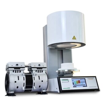
- Versatile Solutions: From induction melting to dental and vacuum furnaces, we cover all high-temp lab needs.
- Expert Customization: Our equipment is tailored to your unique research or production workflows.
Ensure the structural integrity and longevity of your sensors with industry-leading technology. Contact our technical experts today to discuss your application and find the perfect furnace solution!
References
- Simei Zeng, Tao Deng. A Novel High-Temperature Pressure Sensor Based on Graphene Coated by Si<sub>3</sub>N<sub>4</sub>. DOI: 10.1109/jsen.2022.3232626
This article is also based on technical information from Kintek Furnace Knowledge Base .
Related Products
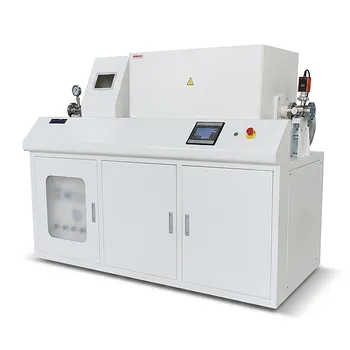
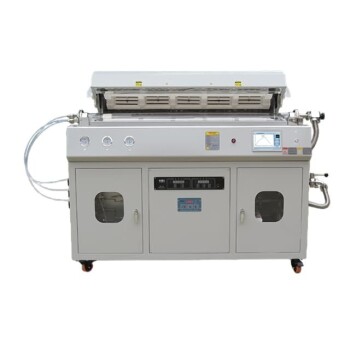
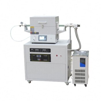
- Slide PECVD Tube Furnace with Liquid Gasifier PECVD Machine
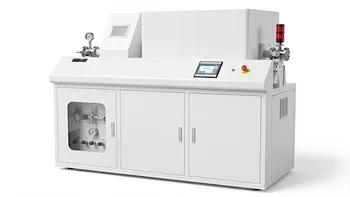
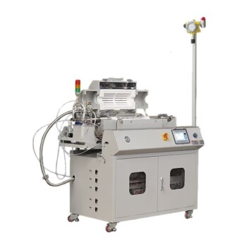
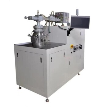
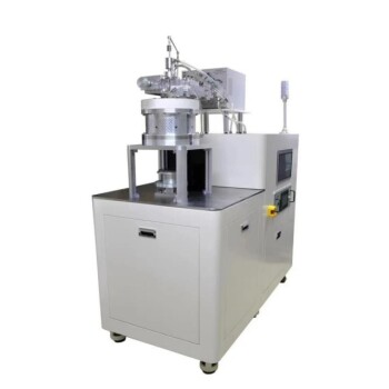
- Inclined Rotary Plasma Enhanced Chemical Deposition PECVD Tube Furnace Machine
- Inclined Rotary Plasma Enhanced Chemical Deposition PECVD Tube Furnace Machine
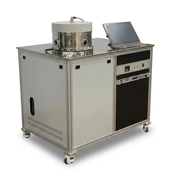
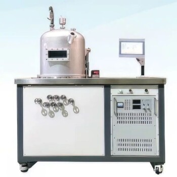
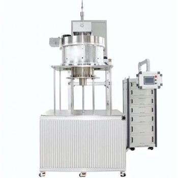
- RF PECVD System Radio Frequency Plasma Enhanced Chemical Vapor Deposition
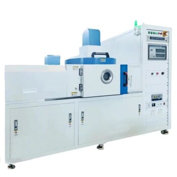
- Multi Heating Zones CVD Tube Furnace Machine for Chemical Vapor Deposition Equipment
People Also Ask
- What are the main advantages of PECVD tube furnaces compared to CVD tube furnaces? Lower Temp, Faster Deposition, and More
- What is plasma in the context of PECVD? Unlock Low-Temperature Thin Film Deposition
- What are the typical conditions for plasma-enhanced CVD processes? Achieve Low-Temperature Thin Film Deposition
- What plasma source is used in PE-CVD tube furnaces? Unlock Low-Temperature, High-Quality Deposition
- What are the advantages of using a tube furnace CVD system for Cu(111)/graphene? Superior Scalability and Quality