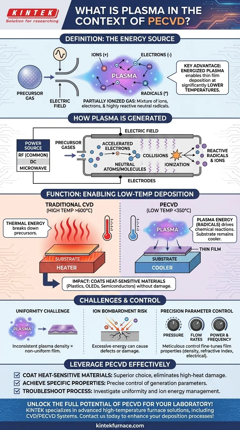
In the context of Plasma-Enhanced Chemical Vapor Deposition (PECVD), plasma is a partially ionized gas that functions as the energy source for the entire deposition process. This gas, composed of a mixture of ions, electrons, and highly reactive neutral radicals, is created by applying an electric field to precursor gases at low pressure. The key advantage is that this energized plasma allows thin films to be deposited at significantly lower temperatures than what is required in conventional methods.
The fundamental role of plasma in PECVD is to replace brute-force thermal energy with targeted chemical energy. This allows complex chemical reactions to occur on a substrate's surface without requiring high, potentially damaging temperatures, broadening the range of materials and devices that can be coated.
How Plasma is Generated in a PECVD System
The Role of the Electric Field
Plasma generation begins by introducing precursor gases into a low-pressure vacuum chamber containing two electrodes. A strong electric field is then applied between these electrodes.
While various power sources can be used, radio frequency (RF) is the most common method for creating a stable and efficient plasma. DC or microwave frequencies are also used for specific applications.
Energizing the Precursor Gas
The applied electric field accelerates free electrons within the chamber to high energy levels. These high-energy electrons then collide with the neutral atoms and molecules of the precursor gas.
Creating a Soup of Reactive Species
These collisions are energetic enough to knock electrons off the gas molecules, creating a cascade of positive ions and more free electrons. This process also breaks chemical bonds, forming highly reactive neutral species called radicals.
This resulting mixture of ions, electrons, radicals, and un-reacted neutral gas molecules is the plasma. It is this collection of reactive species that drives the deposition process.
The Function of Plasma: Enabling Low-Temperature Deposition
Overcoming the Energy Barrier
In traditional Chemical Vapor Deposition (CVD), very high temperatures (often >600°C) are required. This thermal energy is necessary to break down the precursor gas molecules into the atoms that will form the desired film.
Plasma as a Chemical Catalyst
PECVD bypasses the need for extreme heat. The energy required to break down the precursor gases is delivered directly by the energetic plasma, specifically through the creation of radicals.
These radicals are chemically unstable and readily react on the substrate surface to form the thin film. Because the energy is chemical rather than thermal, the substrate itself can remain at a much lower temperature (typically <350°C).
The Impact on Modern Manufacturing
This low-temperature capability is the primary reason PECVD is so valuable. It allows for the deposition of high-quality films on temperature-sensitive materials, such as plastics, organic electronics (OLEDs), and fully fabricated semiconductor devices that would be damaged or destroyed by high-heat processes.
Understanding the Trade-offs and Control
The Challenge of Uniformity
A key engineering challenge in PECVD is generating a perfectly uniform plasma across the entire substrate. Any inconsistency in plasma density or energy will result in a film with non-uniform thickness and properties.
The Risk of Ion Bombardment
While ions are a necessary component of the plasma, excessive bombardment of the substrate surface by high-energy ions can introduce stress, create defects in the film, or even cause physical damage. Managing ion energy is critical for producing high-quality films.
Precision Through Parameter Control
The properties of the final film—such as its density, refractive index, and electrical characteristics—are directly tied to the plasma's characteristics. Experts meticulously control process parameters like gas pressure, gas flow rates, and the power and frequency of the electric field to fine-tune the plasma and, consequently, the deposited material.
How This Applies to Your Deposition Goals
To leverage PECVD effectively, you must understand how plasma directly influences your outcome.
- If your primary focus is coating heat-sensitive materials: PECVD is the superior choice because the plasma provides the reaction energy, eliminating the need for high substrate temperatures that would cause damage.
- If your primary focus is achieving specific film properties: You must precisely control the plasma generation parameters (power, frequency, pressure) to manage the density and type of reactive species being created.
- If you are troubleshooting a PECVD process: Investigate the plasma's uniformity and the potential for damaging ion bombardment, as these are common sources of film defects and poor performance.
Ultimately, mastering PECVD is synonymous with mastering the controlled generation and application of plasma.
Summary Table:
| Aspect | Description |
|---|---|
| Plasma Definition | Partially ionized gas with ions, electrons, and radicals, generated by electric fields at low pressure. |
| Key Advantage | Enables thin film deposition at lower temperatures (<350°C) compared to conventional CVD (>600°C). |
| Generation Method | Typically uses radio frequency (RF) electric fields to energize precursor gases in a vacuum chamber. |
| Main Components | Ions, electrons, radicals, and neutral species that drive chemical reactions on the substrate. |
| Applications | Coating temperature-sensitive materials (e.g., plastics, OLEDs, semiconductors) with high-quality films. |
| Control Parameters | Gas pressure, flow rates, power, and frequency to fine-tune plasma and film properties. |
Unlock the full potential of PECVD for your laboratory! KINTEK specializes in advanced high-temperature furnace solutions, including CVD/PECVD Systems, designed with deep customization to meet your unique experimental needs. Whether you're working with heat-sensitive materials or require precise film properties, our expertise in R&D and in-house manufacturing ensures reliable, efficient results. Contact us today to discuss how we can enhance your deposition processes and achieve superior outcomes!
Visual Guide
Related Products
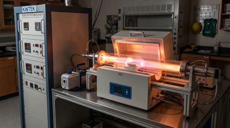
- Slide PECVD Tube Furnace with Liquid Gasifier PECVD Machine
- Inclined Rotary Plasma Enhanced Chemical Deposition PECVD Tube Furnace Machine
- Inclined Rotary Plasma Enhanced Chemical Deposition PECVD Tube Furnace Machine
- Multi Heating Zones CVD Tube Furnace Machine for Chemical Vapor Deposition Equipment
- Split Chamber CVD Tube Furnace with Vacuum Station CVD Machine
People Also Ask
- How does PECVD equipment contribute to TOPCon bottom cells? Mastering Hydrogenation for Maximum Solar Efficiency
- What are the disadvantages of tube furnace cracking when processing heavy raw materials? Avoid Costly Downtime and Inefficiency
- What plasma source is used in PE-CVD tube furnaces? Unlock Low-Temperature, High-Quality Deposition
- How does a hydrogen reduction environment in an industrial tube furnace facilitate gold-copper alloy microspheres?
- In which industries is the tube furnace commonly used? Essential for Materials Science, Energy, and More


