In short, the primary advantage of PECVD is its ability to deposit high-quality thin films at low temperatures. This unique capability, combined with high deposition rates and the versatility to create a wide range of materials, makes Plasma-Enhanced Chemical Vapor Deposition (PECVD) a critical process in industries from semiconductors to medical devices. It effectively overcomes the limitations of traditional, high-heat deposition methods.
The core problem PECVD solves is the need for high-quality, conformal thin films on substrates that cannot withstand high temperatures. By using an energy-rich plasma instead of thermal energy to drive chemical reactions, PECVD decouples film quality from processing temperature, opening up a new range of manufacturing possibilities.
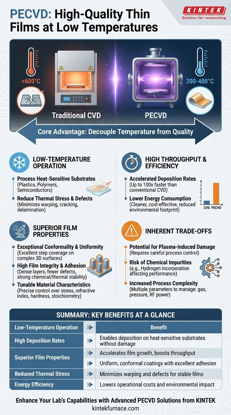
The Core Advantage: Decoupling Temperature from Quality
The most significant benefit of PECVD is its low-temperature operation. This fundamentally changes what is possible in thin-film deposition.
Processing Heat-Sensitive Substrates
Traditional Chemical Vapor Deposition (CVD) often requires temperatures exceeding 600°C. PECVD operates at much lower temperatures, typically 200-400°C.
This makes it possible to deposit films on temperature-sensitive substrates like plastics, polymers, or fully fabricated semiconductor devices that would be damaged or destroyed by high heat.
Reducing Thermal Stress and Defects
High temperatures induce significant thermal stress between the deposited film and the substrate, which can lead to warping, cracking, or delamination.
By operating at lower temperatures, PECVD minimizes this thermal mismatch, resulting in more stable and robust films with a lower risk of mechanical failure.
Achieving High Throughput and Efficiency
Beyond temperature, PECVD is engineered for speed and efficiency, making it highly suitable for manufacturing environments.
Accelerated Deposition Rates
The plasma in a PECVD chamber is a high-energy environment filled with reactive ions and radicals. These species accelerate the chemical reactions needed for film growth far more effectively than heat alone.
This can result in deposition rates that are significantly faster—in some cases, over 100 times faster—than conventional CVD for the same material, directly boosting manufacturing throughput.
Lower Energy Consumption
Eliminating the need for high-temperature furnaces not only protects the substrate but also leads to cleaner and more efficient energy usage. This can translate to lower operational costs and a reduced environmental footprint compared to thermally-intensive processes.
Engineering Superior Film Properties
PECVD provides a remarkable level of control over the final characteristics of the deposited film, allowing for precise material engineering.
Exceptional Conformality and Uniformity
PECVD is known for its ability to produce highly uniform films with excellent step coverage.
This means it can evenly coat complex, non-flat surfaces and three-dimensional geometries, ensuring consistent thickness and performance across an entire substrate.
High Film Integrity and Adhesion
The resulting films exhibit very good adhesion to the substrate. The process produces dense, high-quality layers with fewer defects like pinholes.
This leads to films with high chemical and thermal stability, as well as excellent corrosion and solvent resistance.
Tunable Material Characteristics
PECVD is not a single process but a highly tunable platform. By precisely adjusting parameters like gas composition, pressure, and RF power or frequency, engineers can control the film's final properties.
This allows for fine-tuning of characteristics such as film stress, refractive index, hardness, and stoichiometry (the elemental ratio of compounds), tailoring the material for its specific application.
Understanding the Inherent Trade-offs
While powerful, PECVD is not without its complexities. Acknowledging its trade-offs is key to making an informed decision.
Potential for Plasma-Induced Damage
The same high-energy plasma that enables low-temperature deposition can also cause damage to the substrate surface, particularly in sensitive electronic devices. Careful process control is required to mitigate this risk.
Risk of Chemical Impurities
Because PECVD uses chemical precursors (e.g., silane for silicon films), there is a risk of incorporating unwanted elements, such as hydrogen, into the film. These impurities can negatively affect the film's electrical or optical performance.
Increased Process Complexity
The high degree of "tunability" is a double-edged sword. With more variables to manage—gas flows, pressure, RF power, frequency mixing—developing and maintaining a stable PECVD process can be more complex than simpler deposition techniques like PVD (Physical Vapor Deposition).
Making the Right Choice for Your Goal
Selecting a deposition method depends entirely on your project's specific constraints and desired outcomes.
- If your primary focus is deposition on temperature-sensitive materials: PECVD is often the superior and sometimes only choice over high-temperature CVD.
- If your primary focus is maximum film purity for high-performance electronics: You must carefully evaluate potential hydrogen contamination and plasma damage, sometimes favoring alternative methods like PVD or ALD (Atomic Layer Deposition).
- If your primary focus is high throughput for manufacturing: PECVD's rapid deposition rates provide a significant efficiency advantage for many common films like silicon nitride or oxide.
- If your primary focus is coating complex 3D geometries: PECVD's excellent conformality makes it a strong candidate for ensuring uniform coverage on non-flat surfaces.
By understanding its unique ability to deliver quality without heat, you can leverage PECVD to solve deposition challenges that other methods simply cannot address.
Summary Table:
| Advantage | Key Benefit |
|---|---|
| Low-Temperature Operation | Enables deposition on heat-sensitive substrates like plastics and semiconductors without damage |
| High Deposition Rates | Accelerates film growth, often over 100x faster than traditional CVD, boosting throughput |
| Superior Film Properties | Ensures uniform, conformal coatings with excellent adhesion and tunable characteristics |
| Reduced Thermal Stress | Minimizes warping and defects, leading to more stable and robust films |
| Energy Efficiency | Lowers operational costs and environmental impact by eliminating high-heat requirements |
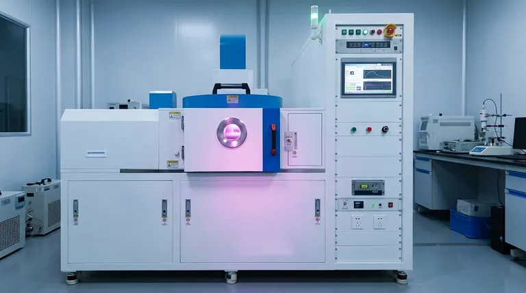
Ready to enhance your lab's capabilities with advanced PECVD solutions? KINTEK leverages exceptional R&D and in-house manufacturing to provide high-temperature furnace solutions tailored for diverse laboratories. Our product line includes Muffle, Tube, Rotary Furnaces, Vacuum & Atmosphere Furnaces, and CVD/PECVD Systems, complemented by strong deep customization to precisely meet your unique experimental needs. Contact us today to discuss how our PECVD systems can deliver high-quality thin films at low temperatures, improve throughput, and solve your deposition challenges!
Visual Guide
Related Products
- Slide PECVD Tube Furnace with Liquid Gasifier PECVD Machine
- RF PECVD System Radio Frequency Plasma Enhanced Chemical Vapor Deposition
- Inclined Rotary Plasma Enhanced Chemical Deposition PECVD Tube Furnace Machine
- Inclined Rotary Plasma Enhanced Chemical Deposition PECVD Tube Furnace Machine
- Multi Heating Zones CVD Tube Furnace Machine for Chemical Vapor Deposition Equipment
People Also Ask
- What is plasma in the context of PECVD? Unlock Low-Temperature Thin Film Deposition
- How does PECVD equipment contribute to TOPCon bottom cells? Mastering Hydrogenation for Maximum Solar Efficiency
- What are the advantages of using a tube furnace CVD system for Cu(111)/graphene? Superior Scalability and Quality
- What are the main advantages of PECVD tube furnaces compared to CVD tube furnaces? Lower Temp, Faster Deposition, and More
- What are the disadvantages of tube furnace cracking when processing heavy raw materials? Avoid Costly Downtime and Inefficiency


