In material manufacturing, the primary advantages of a Chemical Vapor Deposition (CVD) furnace are its ability to produce exceptionally pure, uniform, and durable thin films with precisely controlled properties. This technology enables the creation of advanced materials by depositing coatings with strong adhesion on even the most complex surfaces, enhancing characteristics like hardness, corrosion resistance, and thermal stability.
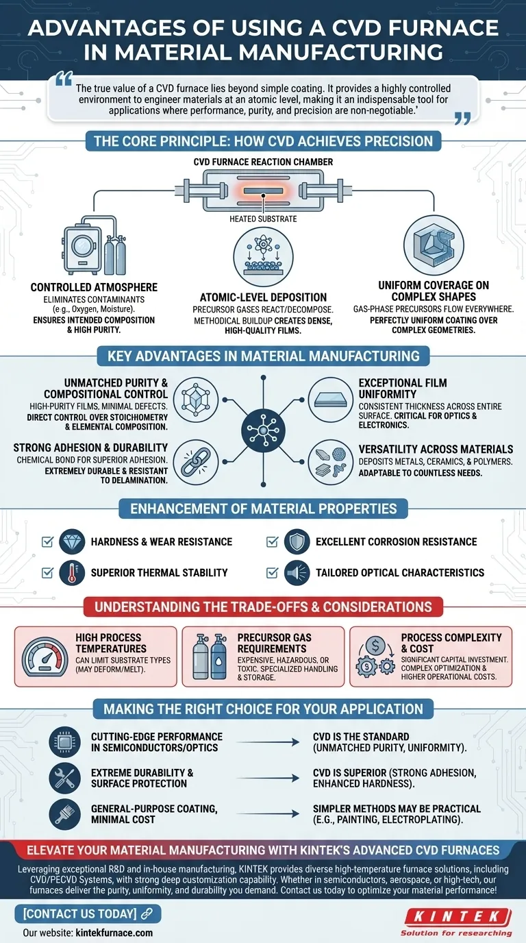
The true value of a CVD furnace lies beyond simple coating. It provides a highly controlled environment to engineer materials at an atomic level, making it an indispensable tool for applications where performance, purity, and precision are non-negotiable.
The Core Principle: How CVD Achieves Precision
A CVD furnace is fundamentally a reaction chamber. Its unique advantages stem directly from its working principle, which transforms gases into a solid, high-performance film on a substrate.
The Role of a Controlled Atmosphere
The entire process takes place in a vacuum or a tightly regulated atmosphere. This clean environment is critical, as it eliminates contaminants like oxygen and moisture that could cause impurities or unwanted side reactions.
This control ensures that the final material's composition is exactly what was intended, resulting in high-purity products with minimal defects.
Atomic-Level Deposition
The process begins by introducing specific precursor gases into the heated furnace chamber. High temperatures cause these gases to chemically react or decompose near the substrate.
This chemical reaction deposits the desired material atom by atom, or molecule by molecule, directly onto the substrate's surface. This methodical buildup is the key to creating dense, high-quality films with excellent structural integrity.
Uniform Coverage on Complex Shapes
Because the precursors are in a gas phase, they can flow and reach every exposed part of the substrate. This allows a CVD furnace to apply a perfectly uniform coating over complex, three-dimensional geometries, a significant challenge for line-of-sight deposition methods like sputtering.
Key Advantages in Material Manufacturing
The unique working principle of CVD translates into several distinct and powerful advantages for producing advanced materials in industries from semiconductors to aerospace.
Unmatched Purity and Compositional Control
The controlled atmosphere prevents contamination, leading to films of exceptionally high purity. By precisely managing the mixture and flow of precursor gases, engineers have direct control over the stoichiometry and elemental composition of the deposited material.
Exceptional Film Uniformity
The gas-phase deposition process ensures that the film's thickness is consistent across the entire surface of the substrate. This uniformity is critical for applications like optics and electronics, where even minor variations can degrade performance.
Strong Adhesion and Durability
Unlike many physical coating methods, CVD creates a chemical bond between the film and the substrate. This results in superior adhesion, making the resulting coatings extremely durable and resistant to delamination.
Versatility Across Materials
CVD is a highly versatile technique capable of depositing a wide range of materials. This includes metals, ceramics (like silicon nitride or titanium carbide), and even some polymers, making it adaptable to countless manufacturing needs.
Enhancement of Material Properties
The primary goal of using CVD is often to impart superior properties to a substrate. These enhancements include drastically improved hardness and wear resistance, superior thermal stability, excellent corrosion resistance, and tailored optical characteristics.
Understanding the Trade-offs and Considerations
While powerful, a CVD furnace is not a universal solution. Its precision comes with specific requirements and limitations that must be weighed against its benefits.
High Process Temperatures
CVD typically requires very high temperatures to initiate the necessary chemical reactions. This can limit the types of substrate materials that can be used, as some may deform or melt under such conditions.
Precursor Gas Requirements
The process is entirely dependent on the availability of suitable precursor gases. These gases can be expensive, hazardous, or toxic, requiring specialized handling, storage, and exhaust management systems.
Process Complexity and Cost
CVD systems are sophisticated and represent a significant capital investment. The process itself can be complex to optimize, and operational costs related to energy, gases, and vacuum systems are often higher than for simpler coating methods.
Making the Right Choice for Your Application
Selecting the right manufacturing process depends entirely on your end goal. A CVD furnace is the definitive choice when performance cannot be compromised.
- If your primary focus is cutting-edge performance in semiconductors or optics: CVD is the standard, as its unmatched purity, uniformity, and compositional control are essential.
- If your primary focus is extreme durability and surface protection: The strong chemical adhesion and enhanced hardness from CVD coatings make it a superior choice for tools, engines, and industrial components.
- If your primary focus is general-purpose coating with minimal cost: Simpler methods like painting or electroplating may be more practical if the absolute highest purity and performance are not required.
Ultimately, adopting CVD is a strategic decision to prioritize material quality and performance above all else.
Summary Table:
| Advantage | Description |
|---|---|
| Unmatched Purity | Controlled atmosphere prevents contamination, ensuring high-purity films with precise composition. |
| Exceptional Uniformity | Gas-phase deposition provides consistent film thickness across complex 3D surfaces. |
| Strong Adhesion | Chemical bonding results in durable, delamination-resistant coatings. |
| Versatility | Capable of depositing metals, ceramics, and polymers for diverse applications. |
| Enhanced Properties | Improves hardness, wear resistance, thermal stability, corrosion resistance, and optical characteristics. |
Elevate Your Material Manufacturing with KINTEK's Advanced CVD Furnaces
Leveraging exceptional R&D and in-house manufacturing, KINTEK provides diverse laboratories with advanced high-temperature furnace solutions. Our product line, including Muffle, Tube, Rotary Furnaces, Vacuum & Atmosphere Furnaces, and CVD/PECVD Systems, is complemented by our strong deep customization capability to precisely meet unique experimental requirements. Whether you're in semiconductors, aerospace, or other high-tech industries, our CVD furnaces deliver the purity, uniformity, and durability your applications demand.
Contact us today to discuss how our tailored solutions can optimize your material performance and efficiency!
Visual Guide
Related Products
- Custom Made Versatile CVD Tube Furnace Chemical Vapor Deposition CVD Equipment Machine
- Split Chamber CVD Tube Furnace with Vacuum Station CVD Machine
- Multi Heating Zones CVD Tube Furnace Machine for Chemical Vapor Deposition Equipment
- Slide PECVD Tube Furnace with Liquid Gasifier PECVD Machine
- Controlled Inert Nitrogen Hydrogen Atmosphere Furnace
People Also Ask
- Which industries and research fields benefit from CVD tube furnace sintering systems for 2D materials? Unlock Next-Gen Tech Innovations
- What are the key application fields of CVD tube furnaces? Unlock Precision in Thin-Film Synthesis
- How does CVD tube furnace sintering enhance graphene growth? Achieve Superior Crystallinity and High Electron Mobility
- What are the practical applications of gate media prepared by CVD tube furnaces? Unlock Advanced Electronics and More
- What future trends are expected in the development of CVD tube furnaces? Discover Smarter, More Versatile Systems


