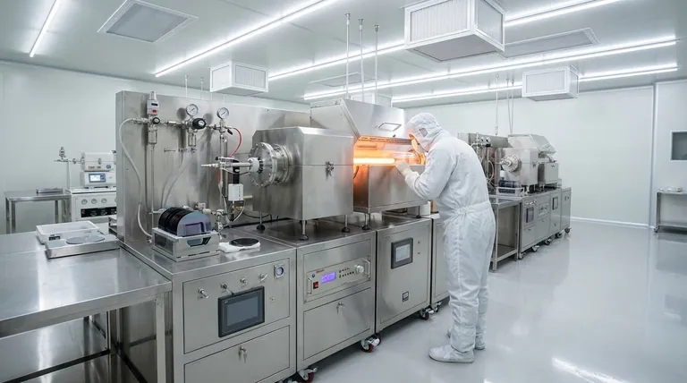
In the semiconductor industry, a Chemical Vapor Deposition (CVD) furnace is a foundational tool used to deposit ultra-thin, high-purity films of material onto silicon wafers. These films, such as silicon dioxide, silicon nitride, and polysilicon, are the essential building blocks used to construct the intricate components of integrated circuits (ICs), transistors, and other microelectronic devices.
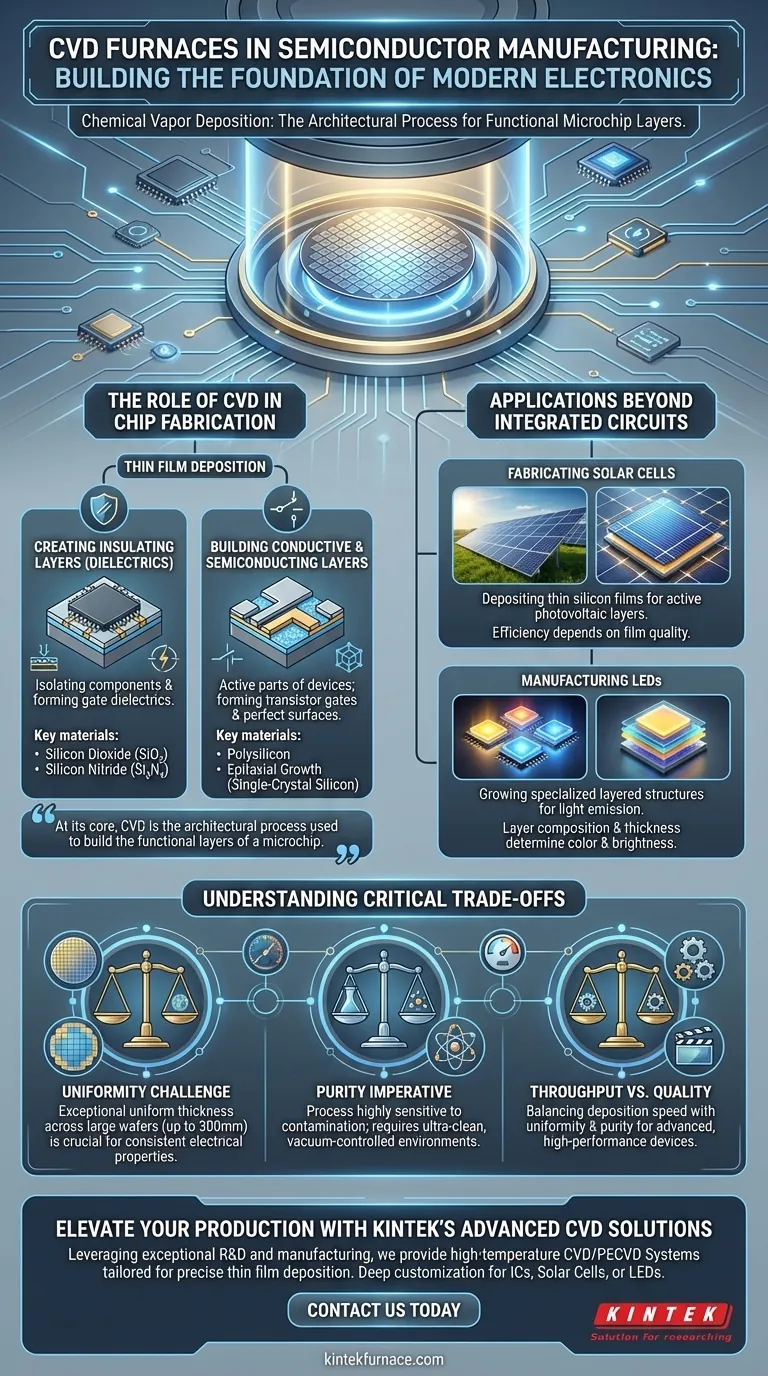
At its core, CVD is not just about coating a surface. It is the architectural process used to build the functional layers of a microchip, creating the insulating, conductive, and semiconducting structures that define modern electronics.
The Role of CVD in Chip Fabrication
The primary function of a CVD furnace in semiconductor manufacturing is thin film deposition. This process involves introducing precursor gases into a high-temperature chamber where they react and decompose, leaving a solid layer of a desired material on the wafer's surface.
Creating Insulating Layers (Dielectrics)
The most common application is depositing dielectric films, which act as insulators. These layers are critical for preventing electrical crosstalk or short circuits between the billions of components on a single chip.
Key materials include silicon dioxide (SiO₂) and silicon nitride (Si₃N₄). They are used to isolate transistors from one another and to form the crucial gate dielectric layer that controls the flow of current within a transistor.
Building Conductive and Semiconducting Layers
CVD is also used to deposit materials that conduct electricity or have semiconductor properties. These layers form the active parts of the electronic devices.
Polysilicon is a primary example, often used to create the "gate" of a transistor—the switch that turns it on and off. Another critical process is epitaxial growth, where CVD is used to grow a perfect, single-crystal layer of silicon on top of the wafer, creating a pristine surface for building high-performance transistors.
Applications Beyond Integrated Circuits
While central to IC manufacturing, the principles of CVD extend to other critical semiconductor-based technologies. The ability to grow uniform, high-quality films is essential for devices that interact with light or generate power.
Fabricating Solar Cells
CVD is widely used to deposit the thin silicon films that form the active photovoltaic layer in solar panels. The efficiency of the solar cell is directly related to the quality and purity of this deposited film.
Manufacturing LEDs
Similarly, the layered structures inside a light-emitting diode (LED) are often grown using a specialized form of CVD. The precise composition and thickness of these deposited layers determine the color and brightness of the light produced.
Understanding the Critical Trade-offs
The value of CVD lies in its precision, but achieving that precision involves managing significant technical challenges. The performance of the final chip is entirely dependent on the quality of these deposited layers.
The Challenge of Uniformity
The deposited film must have an exceptionally uniform thickness across the entire wafer, which can be up to 300mm in diameter. Any slight variation can alter the electrical properties of the device, leading to performance issues or complete failure.
The Purity Imperative
The process is extremely sensitive to contamination. Even trace amounts of unwanted atoms can become embedded in the film, creating defects that destroy the semiconductor's electrical characteristics. This is why CVD is performed in an ultra-clean, vacuum-controlled environment.
Throughput vs. Quality
There is a constant tension between the speed of deposition (throughput) and the quality of the resulting film. Processing wafers faster is more economical, but it can compromise the uniformity and purity required for advanced, high-performance devices.
How to Apply This to Your Goal
The specific CVD application you focus on depends entirely on the component you are trying to create.
- If your primary focus is IC fabrication: The key is using CVD to precisely deposit insulators like SiO₂ and Si₃N₄ and conductors like polysilicon to construct complex transistor architectures.
- If your primary focus is creating foundational wafers: The key process is epitaxial growth of silicon to produce a flawless, single-crystal surface layer required for high-performance electronics.
- If your primary focus is optoelectronics (LEDs/Solar): The key is depositing the specific semiconductor and transparent conductive layers needed to efficiently convert electricity to light or vice-versa.
Ultimately, mastering CVD is a prerequisite for manufacturing virtually any advanced semiconductor device.
Summary Table:
| Application | Key Materials Deposited | Purpose |
|---|---|---|
| IC Fabrication | Silicon Dioxide (SiO₂), Silicon Nitride (Si₃N₄), Polysilicon | Create insulating, conductive layers for transistors and circuits |
| Epitaxial Growth | Single-crystal Silicon | Form high-performance transistor bases |
| Solar Cells | Thin Silicon Films | Enable photovoltaic energy conversion |
| LEDs | Layered Semiconductor Structures | Produce light with specific colors and brightness |
Elevate your semiconductor production with KINTEK's advanced CVD solutions! Leveraging exceptional R&D and in-house manufacturing, we provide high-temperature furnaces like CVD/PECVD Systems tailored for precise thin film deposition. Our deep customization ensures your unique experimental needs are met, whether for ICs, solar cells, or LEDs. Contact us today to discuss how our expertise can optimize your processes and boost efficiency!
Visual Guide
Related Products
- Custom Made Versatile CVD Tube Furnace Chemical Vapor Deposition CVD Equipment Machine
- Split Chamber CVD Tube Furnace with Vacuum Station CVD Machine
- Multi Heating Zones CVD Tube Furnace Machine for Chemical Vapor Deposition Equipment
- Slide PECVD Tube Furnace with Liquid Gasifier PECVD Machine
- Inclined Rotary Plasma Enhanced Chemical Deposition PECVD Tube Furnace Machine
People Also Ask
- How might AI and machine learning enhance CVD tube furnace processes? Boost Quality, Speed, and Safety
- What temperature range do standard CVD tube furnaces operate at? Unlock Precision for Your Material Deposition
- Why are CVD tube furnace sintering systems indispensable for 2D material research and production? Unlock Atomic-Scale Precision
- What are the key application fields of CVD tube furnaces? Unlock Precision in Thin-Film Synthesis
- Which industries and research fields benefit from CVD tube furnace sintering systems for 2D materials? Unlock Next-Gen Tech Innovations


