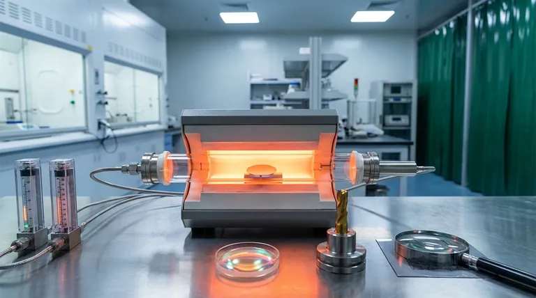
At its core, Chemical Vapor Deposition (CVD) is a foundational manufacturing process used across numerous high-technology fields. It is most commonly applied in the production of semiconductor devices, optical components, advanced materials like carbon nanotubes, and durable, functional coatings for industries ranging from aerospace to biomedical.
The widespread use of CVD is not just about the materials it can create, but how it creates them. Its unique ability to deposit exceptionally pure and uniform thin films over complex, irregular surfaces is what makes it an indispensable tool for modern technology.
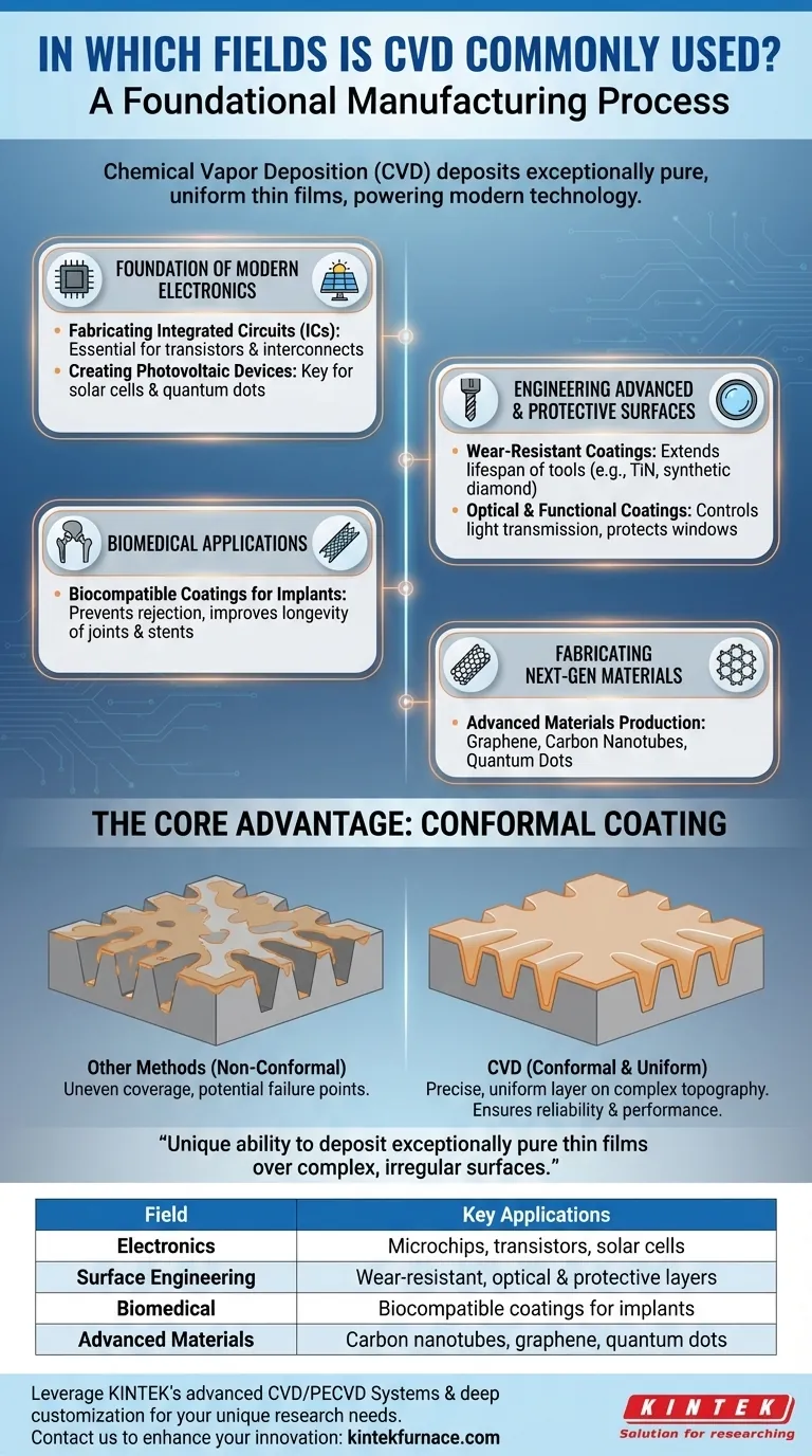
The Foundation of Modern Electronics
CVD is not just a part of the electronics industry; it is the process upon which the entire digital world is built. Its precision at the atomic scale is essential for fabricating microchips.
Fabricating Integrated Circuits (ICs)
Nearly every component inside a microchip, from transistors to interconnects, is built using CVD. The process deposits the ultra-thin, alternating layers of semiconductor, insulating, and metallic materials that form the complex architecture of an integrated circuit.
Creating Photovoltaic Devices
CVD is a key technique for manufacturing solar cells. It is used to deposit the thin films of silicon or other photovoltaic materials (like quantum dots) that capture sunlight and convert it into electricity.
Engineering Advanced and Protective Surfaces
One of CVD's most powerful applications is surface modification, where it imparts new properties to a base material by adding a thin, high-performance layer.
Wear-Resistant Coatings
In demanding mechanical applications, CVD is used to deposit extremely hard coatings, such as titanium nitride or synthetic diamond films, onto cutting tools and engine components. This dramatically increases their lifespan and performance.
Optical and Functional Coatings
CVD creates thin films for optical devices, including anti-reflective coatings on lenses and protective layers on optical windows used in harsh environments. These coatings are precisely engineered to control how light is transmitted or reflected.
Biomedical Applications
For medical implants like artificial joints or stents, biocompatibility is critical. CVD is used to apply inert, biocompatible coatings that prevent rejection by the body and improve the device's longevity.
Understanding the Core Advantage: Conformal Coating
To grasp why CVD is so prevalent, you must understand its primary technical advantage over other deposition methods.
What is a Conformal Coating?
A conformal coating is a film that follows the exact topography of the substrate, covering every peak, valley, and crevice with a layer of uniform thickness. CVD excels at this because the chemical reaction happens everywhere on the surface at once.
Why It Matters
In microelectronics, incomplete coverage of a microscopic trench can cause a circuit to fail. On an aerospace turbine blade, an uneven coating can create a weak point. CVD's ability to create a perfect, conformal film on irregular shapes ensures reliability and performance where other techniques fall short.
How to Apply This Knowledge
Your interest in CVD's applications likely stems from a specific technical or industrial context.
- If your primary focus is electronics manufacturing: Recognize that CVD is the non-negotiable process for building the fundamental layers of virtually all semiconductor devices.
- If your primary focus is material engineering: View CVD as the premier tool for creating high-performance surfaces, enhancing properties like hardness, chemical resistance, or biocompatibility.
- If your primary focus is research and development: Understand that CVD is the gateway to fabricating next-generation materials like graphene, carbon nanotubes, and quantum dots.
Ultimately, understanding where CVD is used is to understand what drives innovation in a vast range of modern technological fields.
Summary Table:
| Field | Key Applications |
|---|---|
| Electronics | Fabrication of microchips, transistors, and solar cells |
| Surface Engineering | Wear-resistant coatings, optical films, and protective layers |
| Biomedical | Biocompatible coatings for implants like stents and joints |
| Advanced Materials | Production of carbon nanotubes, graphene, and quantum dots |
Leveraging exceptional R&D and in-house manufacturing, KINTEK provides diverse laboratories with advanced high-temperature furnace solutions, including CVD/PECVD Systems. Our strong deep customization capability ensures we precisely meet your unique experimental requirements for applications in electronics, coatings, and materials science. Contact us today to enhance your innovation with tailored CVD solutions!
Visual Guide
Related Products
- Custom Made Versatile CVD Tube Furnace Chemical Vapor Deposition CVD Equipment Machine
- Multi Heating Zones CVD Tube Furnace Machine for Chemical Vapor Deposition Equipment
- HFCVD Machine System Equipment for Drawing Die Nano Diamond Coating
- Split Chamber CVD Tube Furnace with Vacuum Station CVD Machine
- 915MHz MPCVD Diamond Machine Microwave Plasma Chemical Vapor Deposition System Reactor
People Also Ask
- What temperature range do standard CVD tube furnaces operate at? Unlock Precision for Your Material Deposition
- Which industries and research fields benefit from CVD tube furnace sintering systems for 2D materials? Unlock Next-Gen Tech Innovations
- How does CVD tube furnace sintering enhance graphene growth? Achieve Superior Crystallinity and High Electron Mobility
- What are the practical applications of gate media prepared by CVD tube furnaces? Unlock Advanced Electronics and More
- Why are CVD tube furnace sintering systems indispensable for 2D material research and production? Unlock Atomic-Scale Precision


