In the electronics and semiconductor industries, furnace brazing is a high-precision thermal process used to create strong, hermetically sealed joints for sensitive components. It is essential for joining materials with different thermal properties, such as ceramics and metals, in a highly controlled environment to prevent contamination and ensure reliability.
The core value of furnace brazing in electronics is not merely joining parts, but manufacturing high-purity, structurally sound components. The controlled atmosphere of the furnace is critical for protecting sensitive materials from oxidation and contamination, which is non-negotiable for semiconductor performance.
The Core Challenge: Joining and Protecting Sensitive Components
Modern electronics rely on combining disparate materials to manage heat, conduct electricity, and provide insulation. Furnace brazing is the solution for creating these complex assemblies with high reliability.
Managing Thermal Expansion
Many electronic packages require joining a ceramic substrate (an insulator) to a metal housing or conductor. These materials expand and contract at different rates when heated.
Furnace brazing excels here by using a filler metal and a precisely controlled heating and cooling cycle. This process minimizes thermal stress, preventing cracks and ensuring a durable, long-lasting bond.
Creating Hermetic Seals
Sensitive electronic and semiconductor components must be protected from moisture, oxygen, and other environmental contaminants.
Furnace brazing is used to create hermetic seals for electronic packaging and sensors. This process ensures the internal microelectronics are completely isolated, which is vital for their performance and longevity.
Key Furnace Processes in Electronics & Semiconductors
Different furnace techniques are applied to achieve specific manufacturing goals, from building up components to bonding entire wafers.
Sintering and Diffusion Bonding
Sintering is a process that uses heat to fuse powdered materials together, forming a solid, high-density component like a ceramic substrate.
Diffusion bonding, often performed in a furnace, joins materials by applying heat and pressure, causing atoms to migrate across the joint interface. Both processes are fundamental to creating high-performance electronic components.
Wafer Bonding
In semiconductor manufacturing, wafer bonding involves joining two or more semiconductor wafers together.
Specialized hot press furnaces apply both uniform heat and pressure in a vacuum to create a perfect, void-free bond between wafers, a critical step in producing advanced microelectronic devices.
Annealing Silicon Wafers
Annealing is a heat treatment process that alters the microstructure of a material to improve its electrical properties and relieve internal stresses.
Vacuum furnaces are used to anneal silicon wafers in a contaminant-free environment. This ensures the crystalline structure is optimized for performance without introducing impurities.
The Critical Role of a Controlled Atmosphere
For both electronics and semiconductors, the environment inside the furnace is just as important as the temperature. The slightest contamination can lead to component failure.
Why a Vacuum is Essential
Most high-end electronic and semiconductor brazing occurs in a vacuum furnace.
A vacuum environment removes oxygen and other reactive gases. This prevents oxidation and contamination of the components and the brazing filler metal, which is absolutely critical for maintaining the purity and electrical integrity of semiconductor materials.
Ensuring Joint Integrity
The clean, controlled atmosphere ensures that the brazing alloy flows cleanly and bonds completely with the parent materials. This results in strong, reliable, and oxidation-free joints essential for the safety and performance of the final product.
Understanding the Trade-offs
While powerful, furnace brazing is a specialized process with specific considerations that make it suitable for high-value applications.
High Initial Investment
Industrial furnaces, particularly high-vacuum or hot-press models, represent a significant capital expense. This cost is justified by the high quality and reliability demanded by the electronics and aerospace industries.
Process Complexity
Furnace brazing is not a simple operation. It requires precise control over temperature profiles, heating and cooling rates, vacuum levels, and material selection to achieve repeatable, high-quality results.
Batch Processing Limitations
Unlike continuous soldering, furnace brazing is typically a batch process. Parts must be loaded into the furnace, the cycle must run, and then the parts must cool before being unloaded. This can impact overall production throughput for very high-volume manufacturing.
Matching the Process to the Application
Your choice of thermal processing technique should be directly tied to the specific requirements of your component.
- If your primary focus is creating robust electronic packages: Furnace brazing is the superior method for creating strong, hermetic seals between ceramic insulators and metal conductors.
- If your primary focus is semiconductor wafer fabrication: A vacuum or hot press furnace is non-negotiable for critical steps like bonding, sintering, and annealing to prevent any form of contamination.
- If your primary focus is joining components with mismatched thermal properties: The controlled heating and cooling cycles of furnace brazing are essential to minimize stress and create a reliable, failure-resistant joint.
Ultimately, mastering controlled thermal processing is fundamental to manufacturing the reliable, high-performance electronics that power our world.
Summary Table:
| Application | Key Benefit | Ideal Furnace Type |
|---|---|---|
| Hermetic Sealing | Protects components from moisture/oxygen | Vacuum Furnace |
| Ceramic-to-Metal Joining | Manages thermal expansion mismatch | Controlled Atmosphere Furnace |
| Wafer Bonding & Annealing | Ensures purity and electrical integrity | Hot Press/Vacuum Furnace |
Need to create reliable, high-purity joints for your electronic or semiconductor components?
At KINTEK, we understand the critical need for contamination-free thermal processing. Our expert R&D and manufacturing team provides customized furnace solutions—including Muffle, Tube, Rotary, Vacuum, and CVD systems—to meet your unique requirements for hermetic sealing, wafer bonding, and precision brazing.
Let us help you achieve superior component performance and longevity. Contact our experts today to discuss your specific application!
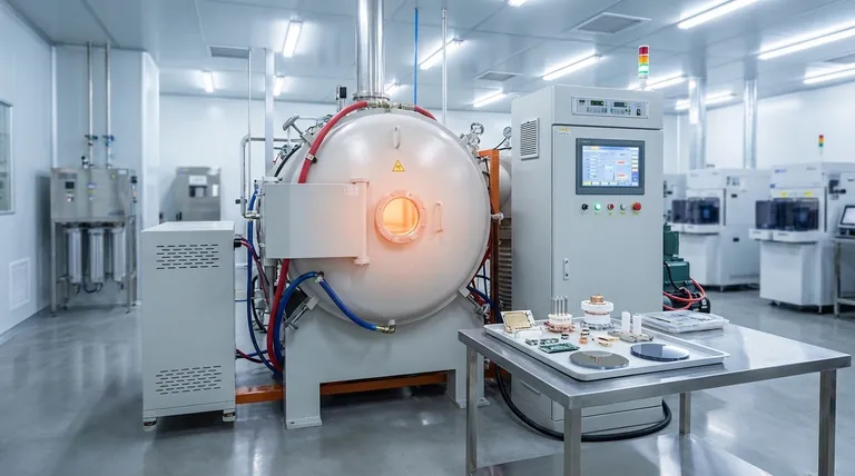
Visual Guide

Related Products
- Vacuum Heat Treat Sintering and Brazing Furnace
- Vacuum Dental Porcelain Sintering Furnace for Dental Laboratories
- High Temperature Muffle Oven Furnace for Laboratory Debinding and Pre Sintering
- Dental Porcelain Zirconia Sintering Ceramic Vacuum Press Furnace
- Small Vacuum Heat Treat and Tungsten Wire Sintering Furnace
People Also Ask
- What are the steps involved in a typical vacuum brazing treatment? Master the Process for Strong, Clean Joints
- What are the benefits of using vacuum heat treating furnaces for metal alloys? Achieve Superior Metal Properties and Performance
- What are the technical advantages of using Ti-35Ni-25Nb foil? High toughness and beta-phase stability.
- What is the significance of vacuum brazing in modern manufacturing? Achieve Strong, Pure Joints for Critical Applications
- What is the temperature of a vacuum furnace brazing? Optimize Your Joint Strength and Cleanliness


