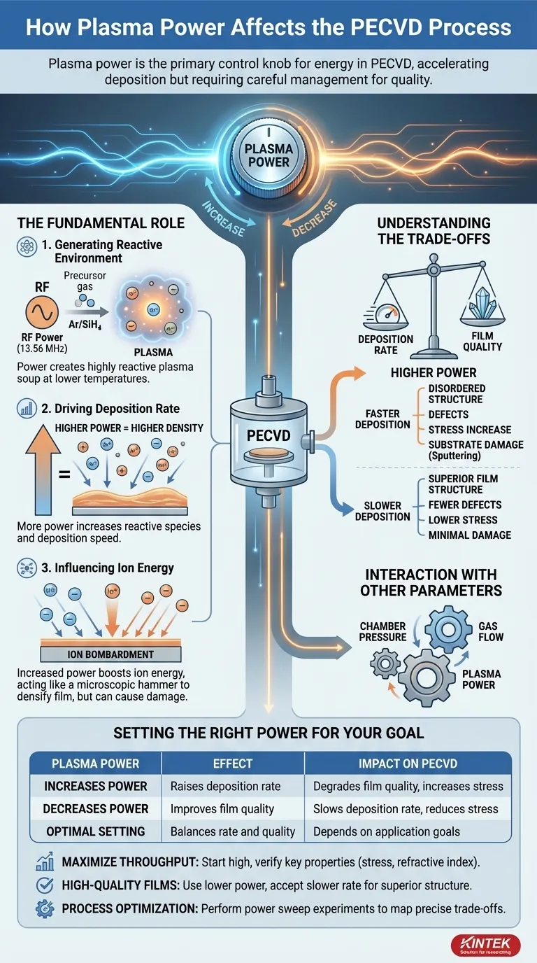
In short, plasma power is the primary control knob for the energy within a PECVD reactor. Increasing power directly raises the density and energy of the plasma, which accelerates the rate of film deposition. However, this increase in energy must be carefully managed, as excessive power can degrade film quality and even damage the substrate.
The core challenge of managing plasma power in PECVD is not simply about turning it up or down. It's about finding the optimal energy "sweet spot" where you achieve a desirable deposition rate without compromising the structural integrity and performance of your thin film.
The Fundamental Role of Plasma Power
To control the PECVD process, you must first understand how plasma power initiates and drives the entire deposition sequence. It is the engine of the reaction.
Generating the Reactive Environment
PECVD systems use an electric field, typically driven by a radio frequency (RF) source at 13.56 MHz, to energize a precursor gas. This applied power strips electrons from gas molecules, creating a partially ionized gas known as plasma. This plasma is a highly reactive soup of ions, electrons, and neutral radical species.
These reactive species are the key to PECVD's advantage, as they allow film-forming chemical reactions to occur at much lower temperatures than in traditional CVD.
Driving the Deposition Rate
The amount of power you apply directly correlates with the density of the plasma. More power creates more ions and radicals per unit volume.
A higher concentration of these reactive species leads to more frequent reactions on the substrate surface, which in turn increases the film's deposition rate. This relationship is one of the most direct and predictable effects of changing power.
Influencing Ion Energy and Bombardment
Beyond just creating reactive species, plasma power also dictates the energy of the ions that bombard the substrate. As power increases, so does the energy with which these ions strike the growing film.
This ion bombardment can be beneficial, acting like a microscopic hammer to "densify" the film and improve its properties. However, as we will see, it is also the primary source of process-related problems.
Understanding the Trade-offs
Using plasma power effectively requires balancing its positive and negative effects. Pushing for one outcome, like speed, will almost always impact another, like quality.
Deposition Rate vs. Film Quality
This is the most critical trade-off. While higher power increases deposition rate, it can also lead to a more disordered film structure.
Excessive ion bombardment can create defects, trap impurities, or alter the film's chemical composition (stoichiometry). The result is often a film with poor optical, electrical, or mechanical properties.
Risk of Substrate Damage
The energetic ions created at high power levels can physically damage the substrate. This is a major concern when depositing films on delicate materials, such as certain semiconductors or polymers.
This damage, known as sputtering or ion-induced damage, can compromise device performance and reliability.
The Impact on Film Stress
Ion bombardment directly influences the internal stress of the deposited film. Typically, higher plasma power leads to an increase in compressive stress.
This "atomic peening" effect can be problematic in applications like MEMS or optics, where high stress can cause film delamination or device deformation. Conversely, it can sometimes be used intentionally to counteract tensile stress.
Interaction with Other Parameters
The effect of plasma power is not isolated. It is deeply interconnected with other process parameters like chamber pressure and gas flow rates.
For instance, at lower pressures, particles have a longer mean free path, and the plasma can behave differently. The same power setting will produce different film properties at 100 mTorr versus 1 Torr, making co-optimization essential.
Setting the Right Power for Your Goal
There is no single "best" power setting; the ideal value depends entirely on your primary objective. Use these guidelines to make a strategic choice.
- If your primary focus is maximizing throughput: Start with a higher power setting to achieve a fast deposition rate, but systematically verify key film properties like stress and refractive index to define your upper process limit.
- If your primary focus is achieving high-quality, defect-free films: Use lower power settings. Accept the slower deposition rate as the necessary trade-off for superior film structure and lower stress.
- If your primary focus is process optimization: Perform a power sweep experiment. Deposit a series of films where only the power is varied, then measure the resulting properties to map out the precise trade-offs for your specific material and system.
Ultimately, mastering plasma power is about using it as a precise tool to engineer the desired film properties for your application.
Summary Table:
| Plasma Power Effect | Impact on PECVD Process |
|---|---|
| Increases Power | Raises deposition rate, but may degrade film quality and increase stress |
| Decreases Power | Improves film quality and reduces stress, but slows deposition rate |
| Optimal Setting | Balances rate and quality; depends on application goals like throughput or defect minimization |
Struggling to optimize plasma power for your PECVD processes? KINTEK specializes in advanced high-temperature furnace solutions, including CVD/PECVD Systems, backed by exceptional R&D and in-house manufacturing. Our deep customization capabilities ensure precise alignment with your unique experimental needs, whether you're focused on maximizing throughput or achieving defect-free films for semiconductors, MEMS, or other applications. Contact us today to enhance your lab's efficiency and film performance!
Visual Guide
Related Products
- Slide PECVD Tube Furnace with Liquid Gasifier PECVD Machine
- RF PECVD System Radio Frequency Plasma Enhanced Chemical Vapor Deposition
- Inclined Rotary Plasma Enhanced Chemical Deposition PECVD Tube Furnace Machine
- Inclined Rotary Plasma Enhanced Chemical Deposition PECVD Tube Furnace Machine
- Multi Heating Zones CVD Tube Furnace Machine for Chemical Vapor Deposition Equipment
People Also Ask
- How does a hydrogen reduction environment in an industrial tube furnace facilitate gold-copper alloy microspheres?
- In which industries is the tube furnace commonly used? Essential for Materials Science, Energy, and More
- How does PECVD equipment contribute to TOPCon bottom cells? Mastering Hydrogenation for Maximum Solar Efficiency
- What are the main advantages of PECVD tube furnaces compared to CVD tube furnaces? Lower Temp, Faster Deposition, and More
- What are the disadvantages of tube furnace cracking when processing heavy raw materials? Avoid Costly Downtime and Inefficiency


