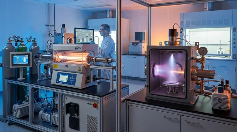
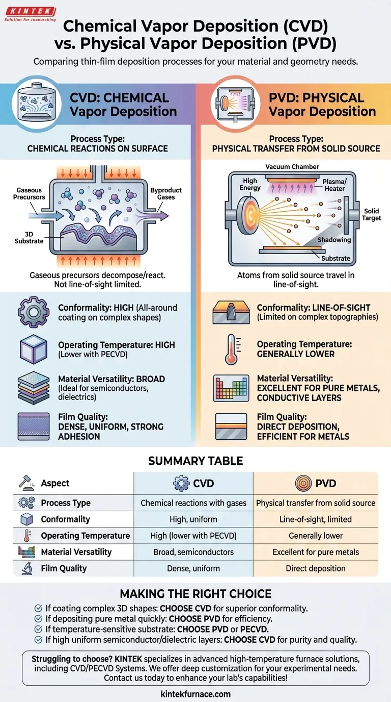
At their core, Chemical Vapor Deposition (CVD) and Physical Vapor Deposition (PVD) are distinguished by their fundamental processes. CVD utilizes chemical reactions on a substrate's surface to grow a film from gaseous precursors, whereas PVD uses physical methods like sputtering or evaporation to transfer material from a solid source to the substrate.
While both CVD and PVD create thin films, your choice hinges on a critical trade-off. CVD uses chemical reactions for highly uniform, all-around coatings, while PVD uses physical force for direct, line-of-sight deposition. Understanding this difference is the key to selecting the right process for your material and geometry.
The Core Mechanisms: Chemical vs. Physical
The names themselves reveal the primary distinction. One process is fundamentally chemical, while the other is physical.
How CVD Works: Gaseous Precursors and Surface Reactions
Chemical Vapor Deposition introduces one or more volatile gaseous precursors into a reaction chamber.
These gases decompose or react on the surface of the heated substrate, forming a solid thin film. The byproduct gases are then exhausted from the chamber.
Because the process is driven by the flow and diffusion of gas, CVD is not limited by line-of-sight. It can uniformly coat complex, non-flat surfaces.
How PVD Works: Solid Sources and Direct Deposition
Physical Vapor Deposition begins with a solid target made of the material you wish to deposit.
High energy, typically from a plasma (sputtering) or a resistive heater (evaporation), bombards this target, dislodging atoms and launching them toward the substrate.
These atoms travel in a straight line and condense on the substrate's surface, creating a line-of-sight deposition. Areas not directly visible to the source material will receive little to no coating.
Comparing Key Process Characteristics
The differences in mechanism lead to significant variations in process outcomes, material compatibility, and film properties.
Deposition Conformality: All-Around vs. Line-of-Sight
The most critical practical difference is conformality—the ability to coat a three-dimensional surface evenly.
CVD excels at this, providing highly conformal films that cover trenches, steps, and complex geometries with uniform thickness.
PVD, being a line-of-sight process, struggles with complex topographies. The tops of features receive a thick coating while the sidewalls receive very little, an effect known as "shadowing."
Operating Temperature and Substrate Compatibility
Traditional CVD processes often require very high temperatures to drive the necessary chemical reactions on the substrate surface. This limits their use to materials that can withstand the heat.
PVD generally operates at lower temperatures, making it more suitable for some temperature-sensitive substrates.
However, a key variant, Plasma-Enhanced CVD (PECVD), uses plasma instead of high heat to energize the precursor gases, allowing for deposition at much lower temperatures (200-400°C).
Material Versatility
PVD is an excellent and widely used method for depositing pure metals and other conductive layers.
CVD offers greater versatility in the types of materials it can deposit. It is the dominant method for creating high-purity semiconductor and dielectric (insulating) films essential for modern electronics.
Understanding the Trade-offs
Neither process is universally superior. The choice involves balancing film quality, process complexity, and compatibility with your goals.
Film Quality and Uniformity
CVD is generally known for producing very precise, dense, and highly uniform thin films. The chemical bonding process results in strong adhesion and excellent film quality.
Variants like PECVD can produce even higher-quality films with a reduced likelihood of cracking compared to some traditional CVD methods.
Process Complexity and Byproducts
CVD equipment can be more complex, and the chemical reactions often produce toxic or corrosive gaseous byproducts that require careful handling and abatement.
PVD is a comparatively cleaner process with minimal environmental impact and simpler equipment, as it is primarily a physical transfer of material in a vacuum.
Making the Right Choice for Your Application
Selecting the correct deposition method requires matching the process capabilities to your end goal.
- If your primary focus is coating complex 3D shapes: Choose CVD for its superior conformality that ensures even coverage on all surfaces.
- If your primary focus is depositing a pure metal film quickly: PVD is often the more direct, efficient, and cost-effective solution.
- If your primary focus is coating a temperature-sensitive substrate like plastic: Your best options are PVD or a low-temperature variant like PECVD.
- If your primary focus is creating highly uniform semiconductor or dielectric layers: CVD is the industry standard for achieving the required purity and film quality.
Ultimately, your decision is guided by the material you need to deposit, the geometry of your substrate, and the final properties your film must possess.
Summary Table:
| Aspect | CVD | PVD |
|---|---|---|
| Process Type | Chemical reactions with gases | Physical transfer from solid source |
| Conformality | High, uniform on complex shapes | Line-of-sight, limited on non-flat surfaces |
| Operating Temperature | High (lower with PECVD) | Generally lower |
| Material Versatility | Broad, ideal for semiconductors | Excellent for pure metals |
| Film Quality | Dense, uniform, strong adhesion | Direct deposition, efficient for metals |
Struggling to choose between CVD and PVD for your thin-film applications? At KINTEK, we specialize in advanced high-temperature furnace solutions, including CVD/PECVD Systems, Muffle, Tube, Rotary, Vacuum & Atmosphere Furnaces. Leveraging exceptional R&D and in-house manufacturing, we offer deep customization to precisely meet your unique experimental requirements, ensuring optimal performance and efficiency. Contact us today to discuss how our tailored solutions can enhance your lab's capabilities and drive your research forward!
Visual Guide
Related Products
- 915MHz MPCVD Diamond Machine Microwave Plasma Chemical Vapor Deposition System Reactor
- Custom Made Versatile CVD Tube Furnace Chemical Vapor Deposition CVD Equipment Machine
- RF PECVD System Radio Frequency Plasma Enhanced Chemical Vapor Deposition
- MPCVD Machine System Reactor Bell-jar Resonator for Lab and Diamond Growth
- HFCVD Machine System Equipment for Drawing Die Nano Diamond Coating
People Also Ask
- In which industries is the microwave plasma chemical vapor deposition system commonly used? Unlock High-Purity Material Synthesis
- What are some key features and benefits of the microwave plasma chemical vapor deposition system? Achieve Unmatched Material Synthesis
- What are the essential components of an MPCVD reactor system? Build a Pristine Environment for High-Purity Materials
- What are the essential components of an MPCVD reactor for diamond film deposition? Unlock High-Quality Diamond Growth
- How does the MPCVD process work to deposit diamond? A Guide to High-Purity Synthesis


