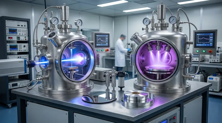
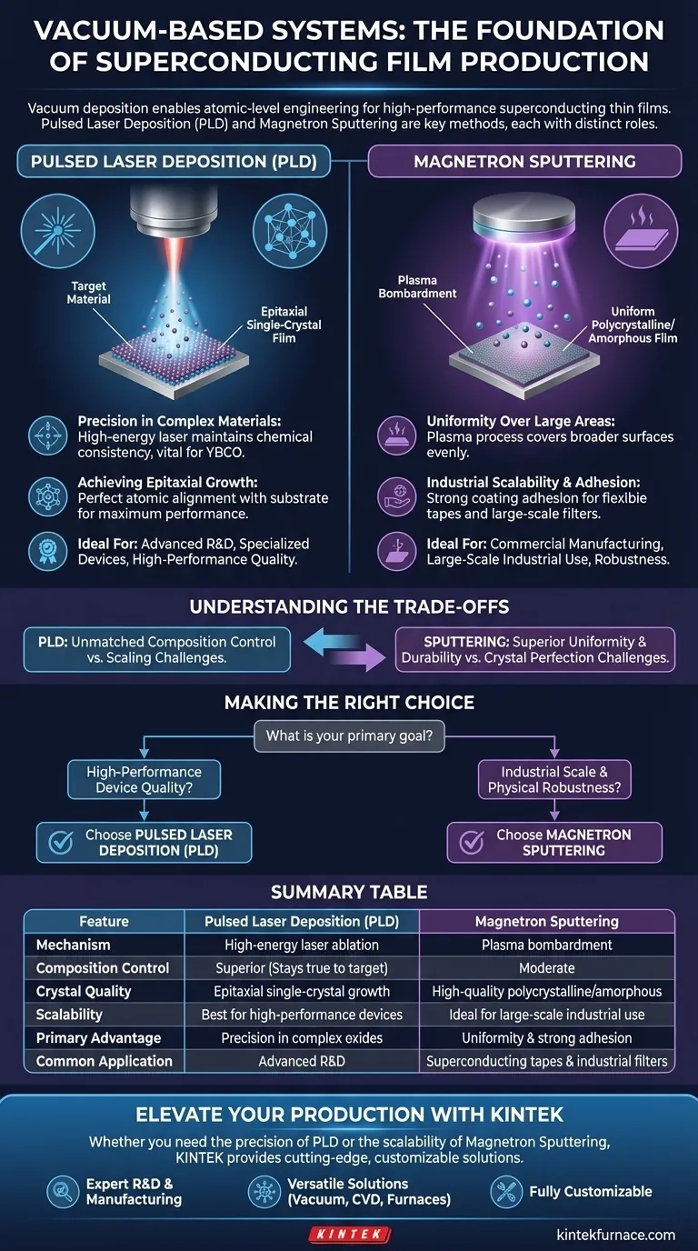
Vacuum-based deposition systems are the cornerstone of modern superconductor manufacturing, enabling the precise atomic-level engineering required for high-performance films. Specifically, Pulsed Laser Deposition (PLD) excels at maintaining complex chemical compositions for high-quality crystal growth, while Magnetron Sputtering provides the uniformity and adhesion necessary for large-scale industrial coatings.
While both technologies operate within vacuum environments to deposit superconducting material, they serve distinct roles: PLD is the premier choice for achieving perfect crystal structures in complex materials, whereas Magnetron Sputtering offers the scalability and physical durability required for commercial manufacturing.
The Role of Pulsed Laser Deposition (PLD)
Precision in Complex Materials
PLD systems utilize high-energy laser beams to ablate (vaporize) target materials. This mechanism is critical because it ensures that the chemical composition of the deposited film remains highly consistent with the target. This is particularly vital when working with complex superconducting materials like YBCO, where maintaining the correct ratio of elements is difficult.
Achieving Epitaxial Growth
The high energy and precise transfer of material allow for the growth of epitaxial single-crystal films. In this context, "epitaxial" means the crystal structure of the film aligns perfectly with the underlying substrate. This structural perfection is essential for maximizing the conductive properties of high-performance superconducting devices.
The Role of Magnetron Sputtering
Uniformity Over Large Areas
Magnetron sputtering systems rely on plasma bombardment to eject atoms from a source material onto a substrate. Unlike the focused nature of a laser, this process is engineered to cover broader areas evenly. It achieves excellent film uniformity, ensuring consistent superconducting properties across the entire surface of the product.
Industrial Scalability and Adhesion
This method creates coatings with strong adhesion, making them physically robust. This durability is a requirement for manufacturing flexible second-generation high-temperature superconducting tapes. It is also the preferred method for producing large-area coatings used in industrial filters, where reliability and scale are paramount.
Understanding the Trade-offs
Composition vs. Coverage
PLD offers unmatched control over chemical stoichiometry, allowing for the creation of perfect crystals from complex oxides. However, the nature of the laser plume can make it challenging to scale this process up for very large surface areas without compromising uniformity.
Durability vs. Crystallinity
Magnetron sputtering excels at producing physically tough, uniform coatings that stick well to flexible substrates. While it is highly effective, it generally faces greater challenges in achieving the same level of atomic-scale crystal perfection that PLD provides for complex compounds.
Making the Right Choice for Your Application
Selecting the right deposition technique requires balancing the need for structural perfection against the requirements of scale and physical durability.
- If your primary focus is high-performance device quality: Choose Pulsed Laser Deposition (PLD) to ensure precise chemical composition and epitaxial single-crystal growth for complex materials like YBCO.
- If your primary focus is industrial scale and physical robustness: Opt for Magnetron Sputtering to achieve the superior film uniformity, strong adhesion, and large-area coverage needed for filters and flexible tapes.
By matching the deposition method to your specific production goals, you ensure the integrity and efficiency of your superconducting systems.
Summary Table:
| Feature | Pulsed Laser Deposition (PLD) | Magnetron Sputtering |
|---|---|---|
| Mechanism | High-energy laser ablation | Plasma bombardment |
| Composition Control | Superior (Stays true to target) | Moderate |
| Crystal Quality | Epitaxial single-crystal growth | High-quality polycrystalline/amorphous |
| Scalability | Best for high-performance devices | Ideal for large-scale industrial use |
| Primary Advantage | Precision in complex oxides (e.g., YBCO) | Uniformity & strong adhesion |
| Common Application | Advanced R&D and specialized devices | Superconducting tapes & industrial filters |
Elevate Your Superconducting Thin Film Production
Precise material deposition is the foundation of high-performance superconductivity. Whether you require the extreme crystal perfection of Pulsed Laser Deposition (PLD) or the industrial-scale uniformity of Magnetron Sputtering, KINTEK provides the cutting-edge technology to achieve your goals.
Why partner with KINTEK?
- Expert R&D & Manufacturing: Our systems are engineered for atomic-level precision.
- Versatile Solutions: From Vacuum and CVD systems to Rotary and Muffle furnaces, we cover all high-temperature lab needs.
- Fully Customizable: We tailor our systems to meet the unique requirements of your specific research or production line.
Contact KINTEK today to discuss your thin-film applications and discover how our customizable vacuum systems can optimize your manufacturing process.
Visual Guide
References
- T. Chattopadhyay. Superconductivity in High-Temperature Materials. DOI: 10.36948/ijfmr.2025.v07i05.55511
This article is also based on technical information from Kintek Furnace Knowledge Base .
Related Products
- RF PECVD System Radio Frequency Plasma Enhanced Chemical Vapor Deposition
- MPCVD Machine System Reactor Bell-jar Resonator for Lab and Diamond Growth
- Slide PECVD Tube Furnace with Liquid Gasifier PECVD Machine
- Inclined Rotary Plasma Enhanced Chemical Deposition PECVD Tube Furnace Machine
- 915MHz MPCVD Diamond Machine Microwave Plasma Chemical Vapor Deposition System Reactor
People Also Ask
- What are some promising applications of PECVD-prepared 2D materials? Unlock Advanced Sensing and Optoelectronics
- What are the applications of plasma enhanced chemical vapor deposition? Key Uses in Electronics, Optics & Materials
- What are the system specifications of the PECVD system? Unlock Precision Thin-Film Deposition
- What are the advantages of PECVD in film deposition? Achieve Low-Temp, High-Quality Coatings
- What is the role of RF power in PECVD and how does the RF-PECVD process work? Master Thin Film Deposition Control


