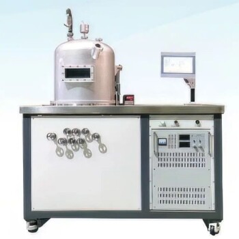
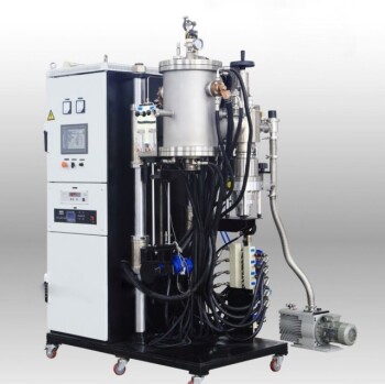
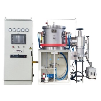
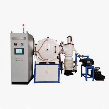
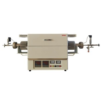
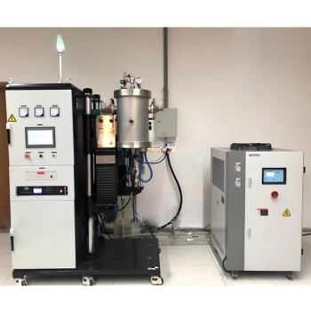
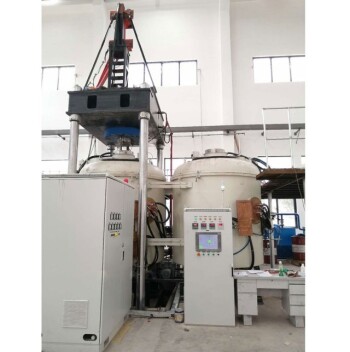
Vacuum evaporation serves as the critical bridge between raw materials and functional electronic devices. To answer your immediate question: this equipment is necessary to deposit metal electrodes (like aluminum or gold) onto graphitic carbon nitride (g-C3N4) with atomic precision, creating a contamination-free interface that allows the metal to bond tightly to the semiconductor surface.
Core Takeaway: The performance of g-C3N4 electronic devices relies entirely on the quality of the metal-semiconductor interface. Vacuum evaporation is the only reliable method to eliminate atmospheric impurities and oxide layers, thereby securing the high-quality Schottky or Ohmic contacts required for accurate electrical characterization.
The Critical Role of the Interface
The primary challenge in fabricating g-C3N4 devices is not just depositing metal, but ensuring that metal interacts correctly with the thin film.
Minimizing Impurities and Oxides
When electrodes are deposited in standard atmospheric conditions, oxygen and airborne particles instantly contaminate the surface.
This creates an unwanted insulating layer or "oxide barrier" between the metal and the carbon nitride.
Vacuum evaporation eliminates this variable. By operating in a vacuum environment, the equipment prevents oxidation and ensures the electrode material remains pure during deposition.
Ensuring Tight Atomic Bonding
For an electronic device to function, electrons must flow freely between the metal electrode and the g-C3N4 film.
This requires physical adhesion at the atomic level.
Vacuum evaporation provides the energy and clean environment necessary for metal atoms to bond tightly with the film surface, creating a mechanically stable and electrically conductive structure.
Electrical Performance Implications
The ultimate goal of using g-C3N4 is to investigate its electronic properties. The deposition method directly dictates whether the resulting data is valid.
Establishing High-Quality Contacts
The nature of the contact—whether Schottky (rectifying) or Ohmic (linear)—defines the device's function.
Vacuum evaporation allows for the precise deposition of specific metals (like Au or Al) to engineer these contacts intentionally.
Without the purity provided by the vacuum, contact resistance increases, distorting electrical signals and reducing device efficiency.
Investigating Rectification Behavior
To understand how g-C3N4 works as a semiconductor, researchers often study its rectification behavior (how it directs current flow).
This analysis requires a pristine junction between the metal and the semiconductor.
Defects or impurities at this interface caused by poor deposition would mimic or mask the intrinsic properties of the material, rendering the investigation of rectification behavior inaccurate.
Understanding the Operational Constraints
While vacuum evaporation is essential for performance, it introduces specific operational requirements that must be managed.
The Requirement for High-Vacuum Levels
This is not a low-precision process; it often requires extremely high vacuum levels (e.g., 4 x 10⁻⁶ Torr).
Achieving and maintaining this pressure is resource-intensive but necessary to prevent environmental impurities from contaminating the layers.
Precision vs. Throughput
The process is designed for meticulous control over film thickness and energy level alignment rather than speed.
You gain high precision and material purity, but you trade away the speed associated with lower-quality deposition methods.
Making the Right Choice for Your Goal
Vacuum evaporation is not optional if your goal is reliable data. Here is how to align this process with your specific objectives:
- If your primary focus is fundamental research: Prioritize vacuum levels that minimize contact resistance to accurately measure the intrinsic rectification behavior of the g-C3N4.
- If your primary focus is device durability: Focus on the vacuum parameters that enhance the physical adhesion and tight bonding of the metal atoms to the film surface.
Ultimately, the integrity of your electronic characterization depends entirely on the purity of the electrode interface established inside the vacuum chamber.
Summary Table:
| Feature | Impact on g-C3N4 Device Performance |
|---|---|
| Vacuum Environment | Prevents oxidation and atmospheric contamination at the interface. |
| Atomic Bonding | Ensures mechanical stability and efficient electron flow between metal/film. |
| Contact Engineering | Enables precise creation of Schottky or Ohmic junctions for data validity. |
| Purity Control | Minimizes contact resistance to accurately measure rectification behavior. |
Elevate Your Material Research with KINTEK Precision
Don't let interface impurities compromise your g-C3N4 research. KINTEK provides high-performance vacuum evaporation systems and laboratory high-temp furnaces designed to deliver the atomic precision your electronic devices demand.
Backed by expert R&D and world-class manufacturing, we offer customizable Muffle, Tube, Rotary, Vacuum, and CVD systems tailored to your unique experimental needs. Ensure the integrity of your electrical characterization today.
Contact KINTEK for a Custom Solution
References
- Kota Higuchi, Yoshio Hashimoto. Layered carbon nitride films deposited under an oxygen-containing atmosphere and their electronic properties. DOI: 10.1063/5.0193419
This article is also based on technical information from Kintek Furnace Knowledge Base .
Related Products
- HFCVD Machine System Equipment for Drawing Die Nano Diamond Coating
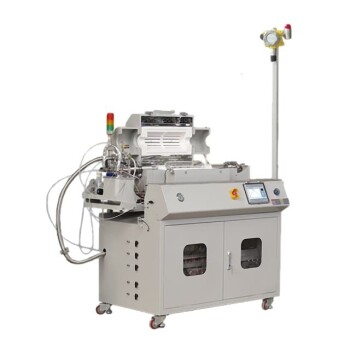
- Multi Heating Zones CVD Tube Furnace Machine for Chemical Vapor Deposition Equipment
- Custom Made Versatile CVD Tube Furnace Chemical Vapor Deposition CVD Equipment Machine
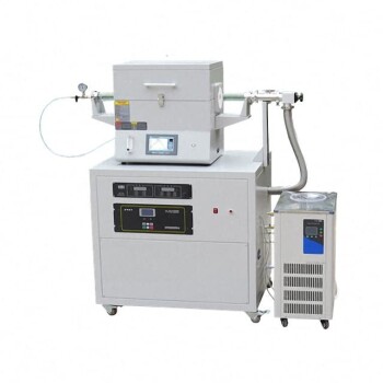
- Split Chamber CVD Tube Furnace with Vacuum Station CVD Machine
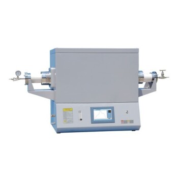
- 1700℃ High Temperature Laboratory Tube Furnace with Alumina Tube
People Also Ask
- What limitations does CVD have in coating large surfaces? Overcome Scale Challenges with Custom Solutions
- How does the availability of specialized furnace systems benefit chemical research? Optimize Your Thermal Processing
- What advantages does the Laser Chemical Vapor Deposition (LCVD) process offer? High Purity & Precision SiC Fibers
- How does a CVD machine work? Master the Technology for High-Quality Thin Film Deposition
- What is a CVD machine? Build High-Performance Materials from Gas with Precision
