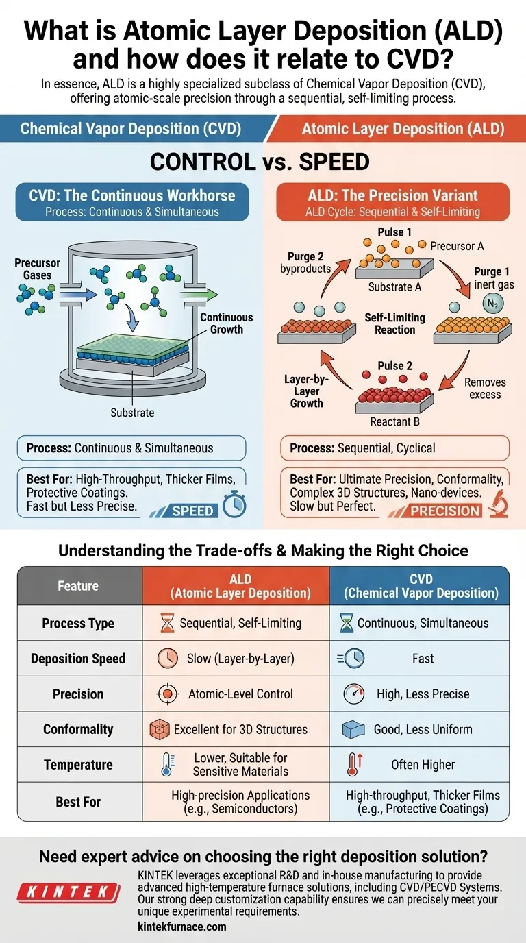
In essence, Atomic Layer Deposition (ALD) is a highly specialized subclass of Chemical Vapor Deposition (CVD). While both techniques are used to create high-quality thin films, ALD provides an unparalleled level of atomic-scale precision by building the film one single layer of atoms at a time. This is achieved through a sequential and self-limiting process, which distinguishes it from the more continuous nature of conventional CVD.
The critical distinction is a matter of control versus speed. CVD is a continuous process that deposits material everywhere at once, making it fast but less precise. ALD is a cyclical process that deposits exactly one atomic layer per cycle, offering ultimate precision and conformity at the cost of speed.
Deconstructing Chemical Vapor Deposition (CVD)
The Core Process
Chemical Vapor Deposition (CVD) is a workhorse process for creating durable, high-performance thin films and coatings. It involves introducing one or more volatile precursor gases into a reaction chamber containing the substrate to be coated.
High temperatures inside the chamber cause the precursor gases to react or decompose. This chemical reaction forms the desired solid material, which then deposits onto all exposed surfaces of the substrate.
Key Characteristics
The deposition in a CVD process is continuous and simultaneous. As long as precursor gases are flowing and the temperature is maintained, the film will continue to grow in thickness across the entire substrate.
This makes CVD a relatively fast and efficient method for producing high-quality films for a wide range of industrial applications, from semiconductors to protective coatings against corrosion and oxidation.
Introducing Atomic Layer Deposition (ALD): The Precision Variant
A Fundamentally Different Approach
ALD is best understood as a more controlled, refined version of CVD. Instead of introducing all precursors at once, ALD uses a sequential, cyclical process.
A typical ALD cycle consists of four distinct steps:
- Pulse 1: The first precursor gas is introduced into the chamber.
- Purge 1: The chamber is purged with an inert gas to remove any unreacted precursor.
- Pulse 2: The second precursor gas (the reactant) is introduced.
- Purge 2: The chamber is purged again to remove reaction byproducts and excess reactant.
The "Self-Limiting" Principle
The genius of ALD lies in its self-limiting reactions. During the first pulse, the precursor molecules can only attach to the available bonding sites on the substrate surface. Once the entire surface is covered (saturated), the reaction stops on its own.
Similarly, the second precursor only reacts with the layer deposited by the first one. This self-limiting nature ensures that exactly one atomic layer of material is deposited per complete cycle.
Unparalleled Control and Conformality
This layer-by-layer growth gives ALD its signature advantages. It enables atomic-level control over film thickness simply by counting the number of cycles performed.
Furthermore, because the precursors are gases that can penetrate anywhere, ALD produces films that are perfectly conformal. They can uniformly coat extremely complex, 3D structures with high aspect ratios, something that is very difficult to achieve with conventional CVD.
Understanding the Trade-offs: ALD vs. CVD
Precision and Film Quality
ALD is the clear winner for precision. Its self-limiting nature produces films with unparalleled thickness control, perfect uniformity, and virtually zero pinholes. CVD films are high-quality but lack this atomic-level perfection.
Deposition Speed
CVD is significantly faster. Because the deposition is continuous, CVD can grow films much more quickly than ALD, which is inherently slowed by its sequential pulse-and-purge cycles. This makes CVD better suited for applications requiring thick films or high throughput.
Temperature
Traditional CVD often requires very high temperatures to drive the chemical reactions. While some variants exist, ALD can typically operate at much lower temperatures. This makes ALD suitable for coating heat-sensitive substrates like plastics or organic materials.
Making the Right Choice for Your Goal
Ultimately, the choice between ALD and CVD depends entirely on your project's specific requirements.
- If your primary focus is ultimate precision and conformality: ALD is the only choice, especially for advanced semiconductor devices, nano-structures, and complex 3D components.
- If your primary focus is high throughput and cost-efficiency for thicker films: CVD is the superior option, ideal for general protective coatings, optics, and solar cells.
- If your primary focus is coating a temperature-sensitive material: ALD's lower processing temperature gives it a distinct advantage over many traditional CVD processes.
Choosing the right deposition technique requires balancing the need for perfection against the practical demands of speed and throughput.
Summary Table:
| Feature | ALD | CVD |
|---|---|---|
| Process Type | Sequential, self-limiting | Continuous, simultaneous |
| Deposition Speed | Slow (layer-by-layer) | Fast |
| Precision | Atomic-level control | High, but less precise |
| Conformality | Excellent for 3D structures | Good, but less uniform |
| Temperature | Lower, suitable for sensitive materials | Often higher |
| Best For | High-precision applications (e.g., semiconductors) | High-throughput, thicker films (e.g., protective coatings) |
Need expert advice on choosing the right deposition solution for your lab? KINTEK leverages exceptional R&D and in-house manufacturing to provide advanced high-temperature furnace solutions, including CVD/PECVD Systems. Our strong deep customization capability ensures we can precisely meet your unique experimental requirements, whether you're working with semiconductors, protective coatings, or other applications. Contact us today to discuss how our tailored solutions can enhance your research and development!
Visual Guide
Related Products
- RF PECVD System Radio Frequency Plasma Enhanced Chemical Vapor Deposition
- HFCVD Machine System Equipment for Drawing Die Nano Diamond Coating
- MPCVD Machine System Reactor Bell-jar Resonator for Lab and Diamond Growth
- Custom Made Versatile CVD Tube Furnace Chemical Vapor Deposition CVD Equipment Machine
- Inclined Rotary Plasma Enhanced Chemical Deposition PECVD Tube Furnace Machine
People Also Ask
- How is silicon dioxide deposited from tetraethylorthosilicate (TEOS) in PECVD? Achieve Low-Temperature, High-Quality SiO2 Films
- How does film quality compare between PECVD and CVD? Choose the Best Method for Your Substrate
- How are deposition rates and film properties controlled in PECVD? Master Key Parameters for Optimal Thin Films
- What are the advantages of PECVD in film deposition? Achieve Low-Temp, High-Quality Coatings
- What is RF in PECVD? A Critical Control for Plasma Deposition


