The primary purpose of the ultra-thin ruthenium (Ru) buffer layer is to act as a structural bridge between the sapphire substrate and the Ru50Mo50 thin film. By depositing this layer—which is approximately 0.7 nm thick—you effectively manage the lattice mismatch and significantly reduce the interfacial stress that typically occurs when dissimilar materials are combined.
Core Takeaway Direct deposition of Ru50Mo50 onto sapphire can lead to structural defects due to atomic misalignment. The Ru buffer layer functions as a foundational template, optimizing the epitaxial orientation to ensure the subsequent film forms a high-quality hexagonal close-packed (hcp) structure.
The Mechanics of Interface Engineering
Managing Lattice Mismatch
When you deposit a film onto a substrate, the atoms of the two materials rarely line up perfectly. This difference in atomic spacing is known as lattice mismatch.
The ultra-thin Ru buffer layer serves to accommodate this difference. It prevents the structural disjoints from propagating directly into the functional Ru50Mo50 layer.
Reducing Interfacial Stress
Lattice mismatch generates significant stress at the interface between the substrate and the film. Left unchecked, this stress can lead to defects or poor film adhesion.
The 0.7 nm Ru layer absorbs and mitigates this stress. This creates a more stable foundation for the subsequent layers to grow upon.
Optimizing Crystalline Quality
Inducing Epitaxial Orientation
For a thin film to perform well, its crystalline orientation must be uniform. The buffer layer acts as a guide for the atoms of the Ru50Mo50 film.
It induces the correct epitaxial orientation right from the start of the growth process. This ensures that the film grows in a predictable and ordered manner.
Ensuring High-Quality HCP Structure
The target structure for the Ru50Mo50 film is hexagonal close-packed (hcp). Achieving a pristine hcp structure is difficult without a proper template.
The Ru buffer optimizes the crystalline quality of the 10 nm Ru50Mo50 layer. It ensures the final film maintains a high-quality hcp structure throughout its volume.
Understanding the Trade-offs
Precision Requirements
While the buffer layer solves structural problems, it introduces a requirement for extreme precision.
The layer is only ~0.7 nm thick. Deviations in this thickness could fail to provide adequate stress relief or potentially disrupt the epitaxial template.
Process Complexity
Adding a buffer layer introduces an additional step to the fabrication process.
You must carefully control the deposition parameters to ensure this ultra-thin layer is continuous and uniform before the main film is deposited.
Making the Right Choice for Your Goal
When designing thin film stacks involving Ru50Mo50 and sapphire, consider your specific performance metrics:
- If your primary focus is Structural Integrity: The buffer layer is non-negotiable for reducing interfacial stress and preventing delamination.
- If your primary focus is Electronic/Magnetic Performance: The buffer is essential because high-quality epitaxial orientation (hcp) is usually a prerequisite for consistent material properties.
Ultimately, the inclusion of this ultra-thin buffer is a precise engineering decision to sacrifice a small amount of process simplicity for a massive gain in crystalline perfection.
Summary Table:
| Feature | Ru Buffer Layer (0.7 nm) | Impact on Ru50Mo50 Film |
|---|---|---|
| Function | Structural Template | Induces epitaxial orientation |
| Stress Relief | Mitigates Lattice Mismatch | Reduces defects and improves adhesion |
| Crystal Structure | Hexagonal Close-Packed (hcp) | Ensures high-quality hcp formation |
| Thickness | Ultra-thin (~0.7 nm) | Minimal volume with maximum stability |
Elevate Your Material Research with KINTEK
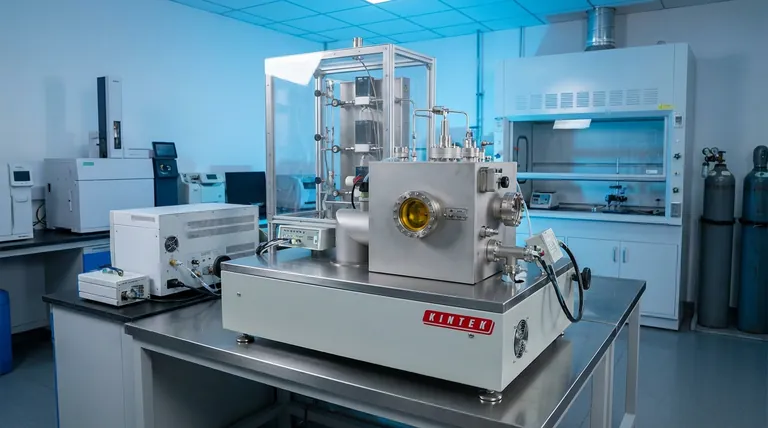
Precision at the atomic level requires high-performance equipment. Whether you are engineering ultra-thin buffer layers or complex thin film stacks, KINTEK provides the specialized tools needed for crystalline perfection.
Backed by expert R&D and manufacturing, we offer Muffle, Tube, Rotary, Vacuum, and CVD systems, all customizable to your unique research and industrial needs. Our high-temperature furnace solutions ensure the thermal stability and precision required for advanced interface engineering.
Ready to optimize your thin film deposition? Contact our experts today to discuss your custom furnace requirements and enhance your lab's efficiency.
References
- Ke Tang, Seiji Mitani. Enhanced orbital torque efficiency in nonequilibrium Ru50Mo50(0001) alloy epitaxial thin films. DOI: 10.1063/5.0195775
This article is also based on technical information from Kintek Furnace Knowledge Base .
Related Products
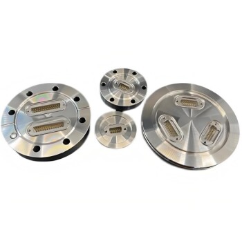
- High Performance Vacuum Bellows for Efficient Connection and Stable Vacuum in Systems
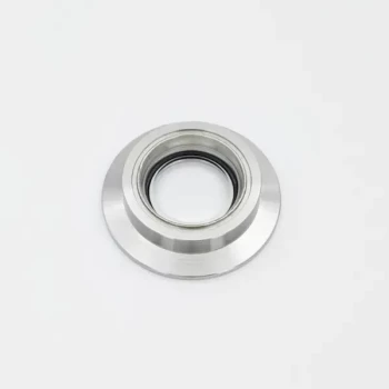
- Ultra High Vacuum CF Observation Window Flange with High Borosilicate Glass Sight Glass
- Stainless Steel Quick Release Vacuum Chain Three Section Clamp
- CF KF Flange Vacuum Electrode Feedthrough Lead Sealing Assembly for Vacuum Systems
- Multi Heating Zones CVD Tube Furnace Machine for Chemical Vapor Deposition Equipment
People Also Ask
- Why are micrometer-scale micro-fiber filter candles used to treat condensed flue gases in pyrolysis systems?
- How does the pressure environment affect the metallic thermal reduction for titanium? Master Precision Control
- Why is an Ultra-High Vacuum (UHV) System Required for In2Se3? Achieving Atomic-Level Ferroelectric Clarity
- What role does a closed pressure vessel play during the carbonation of gamma-C2S? Unlock Rapid Mineralization
- Why is rapid quenching required during the preparation of amorphous glass fertilizers? Boost Nutrient Solubility