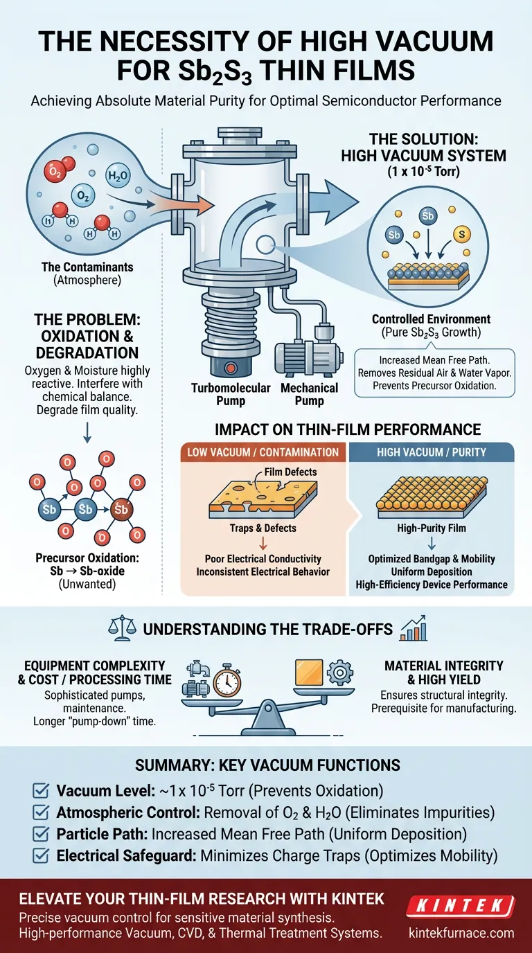
The necessity of a high vacuum pumping system in Sb2S3 preparation stems from the critical requirement for absolute material purity. A vacuum level of approximately 1 x 10^-5 Torr effectively removes atmospheric contaminants like oxygen and moisture that would otherwise degrade the film. This controlled environment ensures that the chemical reaction remains stable, preventing the precursor materials from oxidizing and compromising the semiconductor's final electrical properties.
High vacuum systems serve as the primary safeguard against the oxidation of metallic antimony precursors during the thin-film deposition and sulfurization process. By eliminating residual air and moisture, these systems preserve the stoichiometric integrity and electrical performance of the antimony trisulfide semiconductor.
The Role of Vacuum in Maintaining Chemical Purity
Eliminating Atmospheric Contaminants
Before the sputtering or thermal treatment begins, the chamber must be cleared of residual air and water vapor. These elements are highly reactive and can interfere with the delicate chemical balance required for high-quality film growth.
Achieving a high vacuum ensures that the mean free path of particles is increased, reducing the likelihood of unwanted collisions. This allows the target atoms to reach the substrate without incorporating atmospheric impurities.
Preventing Precursor Oxidation
Antimony (Sb) precursors are particularly sensitive to oxygen during the deposition phase. Without a high vacuum, the metallic antimony would undergo unwanted oxidation, turning into an oxide rather than the intended trisulfide.
This oxidation process is detrimental because it alters the chemical composition of the material. A high vacuum environment ensures that the sulfurization process occurs correctly, resulting in a pure Sb2S3 layer.
Impact on Thin-Film Performance
Protecting Electrical Conductivity
The presence of oxides or moisture within the thin film creates defects that hinder the flow of charge carriers. By maintaining a vacuum of 1 x 10^-5 Torr, the system prevents these "traps" from forming in the semiconductor lattice.
High-purity films exhibit the specific bandgap and mobility characteristics required for efficient device performance. This is especially critical for applications in photovoltaics or sensors where electrical efficiency is paramount.
Ensuring Uniform Deposition
A high vacuum provides a consistent and reproducible environment for thermal treatment. This stability allows for the growth of a homogenous thin film with uniform thickness and grain structure across the entire substrate.
Variations in the vacuum level can lead to localized impurities, which result in inconsistent electrical behavior. Precise vacuum control is therefore a prerequisite for high-yield manufacturing.
Understanding the Trade-offs
Equipment Complexity and Cost
Maintaining high vacuum levels requires sophisticated pumping stations, typically involving a combination of mechanical and turbomolecular pumps. These systems increase the initial capital investment and require rigorous maintenance to prevent leaks.
Processing Time
Achieving a deep vacuum adds significant "pump-down" time to the fabrication cycle. While this reduces throughput, it is a necessary trade-off to ensure the structural integrity of the semiconductor material.
Optimizing the Vacuum Environment for Your Project
When preparing Sb2S3 thin films, your vacuum strategy should align with your specific performance requirements.
- If your primary focus is high electrical efficiency: You must prioritize achieving a deep vacuum of at least 1 x 10^-5 Torr to eliminate all traces of oxygen-related defects.
- If your primary focus is rapid prototyping: You may use a slightly lower vacuum for initial tests, but you must accept the risk of higher impurity levels and reduced film stability.
- If your primary focus is material longevity: Ensure the vacuum system is integrated with an inert gas purge to prevent oxidation during the cooling phase post-thermal treatment.
A robust high vacuum system is not merely an accessory but the fundamental framework required to unlock the full semiconductor potential of antimony trisulfide.
Summary Table:
| Vacuum Requirement | Key Function | Impact on Sb2S3 Performance |
|---|---|---|
| Vacuum Level | ~1 x 10^-5 Torr | Prevents oxidation of metallic antimony precursors |
| Atmospheric Control | Removal of O2 and H2O | Eliminates chemical impurities and lattice defects |
| Particle Path | Increased Mean Free Path | Ensures uniform deposition and stoichiometric integrity |
| Electrical Safeguard | Minimizes Charge Traps | Optimizes bandgap and mobility for photovoltaics |
Elevate Your Thin-Film Research with KINTEK
Precise vacuum control is the difference between a failing device and a high-efficiency semiconductor. Backed by expert R&D and manufacturing, KINTEK offers high-performance Vacuum, CVD, and thermal treatment systems specifically engineered for sensitive material synthesis.
Whether you are preparing Sb2S3, advanced solar cells, or custom semiconductors, our systems provide the stability and purity your project demands. Unlock the full potential of your materials with our customizable high-temperature furnace solutions.
Contact KINTEK today to discuss your vacuum system needs
Visual Guide
References
- Sheyda Uc-Canché, Juan Luis Ruiz de la Peña. Influence of Sulfurization Time on Sb2S3 Synthesis Using a New Graphite Box Design. DOI: 10.3390/ma17071656
This article is also based on technical information from Kintek Furnace Knowledge Base .
Related Products
- High Performance Vacuum Bellows for Efficient Connection and Stable Vacuum in Systems
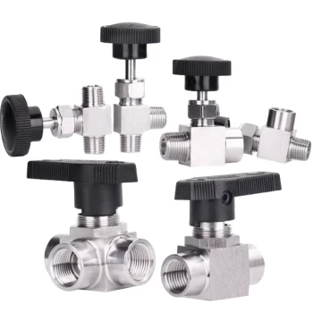
- 304 316 Stainless Steel High Vacuum Ball Stop Valve for Vacuum Systems
- HFCVD Machine System Equipment for Drawing Die Nano Diamond Coating
People Also Ask
- Why is rapid quenching required during the preparation of amorphous glass fertilizers? Boost Nutrient Solubility
- How does a Mass Flow Controller influence 2D superlattices? Precision CVD Control for Sub-10nm Patterning
- What role does a mass flow controller (MFC) play in gas distribution? Ensure Precision in Sensor Performance Evaluation
- Why is an environmental laboratory chamber equipped with an optical window required for synthesizing Hafnium Carbide?
- How does the pressure environment affect the metallic thermal reduction for titanium? Master Precision Control