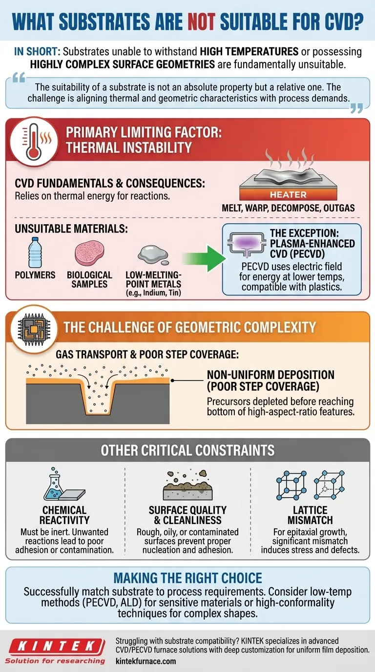
In short, substrates that cannot withstand high temperatures or that possess highly complex surface geometries are fundamentally unsuitable for many standard Chemical Vapor Deposition (CVD) processes. The primary failure points are thermal degradation of the substrate itself and the inability to form a uniform, consistent film over intricate features.
The suitability of a substrate is not an absolute property but a relative one. The central challenge is aligning the substrate's thermal and geometric characteristics with the specific temperature, chemical, and gas flow demands of the chosen CVD process.
The Primary Limiting Factor: Thermal Instability
Chemical Vapor Deposition fundamentally relies on thermal energy to drive the chemical reactions that form the desired film. This high-temperature requirement immediately disqualifies materials that cannot maintain their structural integrity under such conditions.
Understanding CVD's High-Temperature Environment
Most conventional CVD processes, such as thermal CVD, operate at temperatures ranging from a few hundred to over a thousand degrees Celsius. This heat is necessary to break down the precursor gases and enable them to react and deposit onto the substrate surface.
The Consequences of Thermal Sensitivity
When a substrate is heated beyond its stability point, it can melt, decompose, warp, or outgas. This not only destroys the substrate but also contaminates the reaction chamber and prevents the formation of a usable film.
Materials like most polymers, biological samples, or low-melting-point metals (e.g., indium, tin) are classic examples of thermally unsuitable substrates for standard CVD.
The Exception: Lower-Temperature CVD Variants
It is critical to note that variants like Plasma-Enhanced CVD (PECVD) were developed specifically to address this limitation. PECVD uses an electric field to create a plasma, providing the energy for the reaction at much lower temperatures, often making it compatible with temperature-sensitive materials like plastics.
The Challenge of Geometric Complexity
The second major barrier is physical. CVD relies on precursor gases flowing over and diffusing to the substrate surface. Complex topographies can disrupt this process, leading to inconsistent and unreliable film deposition.
The Principle of Gas Transport
For a film to form, precursor molecules must travel from the gas phase to every part of the substrate's surface. This journey is influenced by gas pressure, flow dynamics, and the physical "line of sight" to the surface.
Why Complex Shapes Cause Problems
Substrates with high-aspect-ratio features, such as deep trenches or microscopic holes, pose a significant challenge. The precursor gases may be depleted before they can reach the bottom of these features, a problem known as poor step coverage or conformality.
The Result: Non-Uniform Deposition
This gas depletion leads to a film that is thick at the top opening of a feature but thin or non-existent at the bottom. This non-uniformity compromises the electrical, mechanical, or optical properties of the final device, rendering it ineffective.
Understanding the Trade-offs and Other Constraints
Beyond heat and geometry, other subtle but critical factors can make a substrate unsuitable for a specific CVD application.
Chemical Reactivity
The substrate must be chemically inert with respect to the precursor gases and the deposited film at the process temperature. Unwanted reactions can lead to poor film adhesion, the formation of an undesirable interface layer, or contamination of the film itself.
Surface Quality and Cleanliness
CVD is highly sensitive to the condition of the substrate surface. A surface that is rough, oily, or contaminated with particles will prevent proper nucleation and growth. This results in poor adhesion and a defective film structure.
Lattice Mismatch
In advanced applications like epitaxial growth, where a single-crystal film is grown, the substrate must have a similar crystal lattice structure to the film. A significant lattice mismatch induces stress and defects, disrupting the desired crystalline quality.
Making the Right Choice for Your Process
Selecting a substrate requires a clear understanding of your deposition method and final goal.
- If your substrate is temperature-sensitive: Explore low-temperature deposition techniques like Plasma-Enhanced CVD (PECVD) or Atomic Layer Deposition (ALD).
- If your substrate has complex geometry: Investigate methods known for high conformality, such as ALD, or carefully optimize CVD process parameters (pressure, temperature, flow rates) to improve step coverage.
- If your primary issue is film quality or adhesion: Scrutinize the substrate for potential chemical reactivity with your precursors and ensure its surface is impeccably cleaned and prepared before deposition.
Ultimately, successful deposition is achieved by thoughtfully matching the substrate to the precise requirements of the process.
Summary Table:
| Limiting Factor | Description | Examples of Unsuitable Substrates |
|---|---|---|
| Thermal Instability | Substrates that degrade at high CVD temperatures (e.g., melting, warping) | Polymers, biological samples, low-melting-point metals (e.g., indium, tin) |
| Geometric Complexity | Substrates with intricate features that hinder uniform gas flow and film deposition | High-aspect-ratio structures like deep trenches and microscopic holes |
| Other Constraints | Issues like chemical reactivity, poor surface quality, or lattice mismatch | Rough, contaminated surfaces; chemically reactive materials; mismatched crystals for epitaxy |
Struggling with substrate compatibility in your CVD processes? KINTEK specializes in advanced high-temperature furnace solutions, including CVD/PECVD systems, tailored for diverse laboratory needs. Leveraging our exceptional R&D and in-house manufacturing, we offer deep customization to overcome thermal and geometric challenges, ensuring uniform film deposition and enhanced experimental outcomes. Contact us today to discuss how our Muffle, Tube, Rotary, Vacuum & Atmosphere Furnaces, and CVD/PECVD Systems can optimize your lab's efficiency and success!
Visual Guide
Related Products
- Custom Made Versatile CVD Tube Furnace Chemical Vapor Deposition CVD Equipment Machine
- HFCVD Machine System Equipment for Drawing Die Nano Diamond Coating
- Multi Heating Zones CVD Tube Furnace Machine for Chemical Vapor Deposition Equipment
- Split Chamber CVD Tube Furnace with Vacuum Station CVD Machine
- Slide PECVD Tube Furnace with Liquid Gasifier PECVD Machine
People Also Ask
- Why are CVD tube furnace sintering systems indispensable for 2D material research and production? Unlock Atomic-Scale Precision
- How might AI and machine learning enhance CVD tube furnace processes? Boost Quality, Speed, and Safety
- How can integrating CVD tube furnaces with other technologies benefit device fabrication? Unlock Advanced Hybrid Processes
- What is a CVD tube furnace and what is its primary function? Discover Precision Thin-Film Deposition
- What future trends are expected in the development of CVD tube furnaces? Discover Smarter, More Versatile Systems


