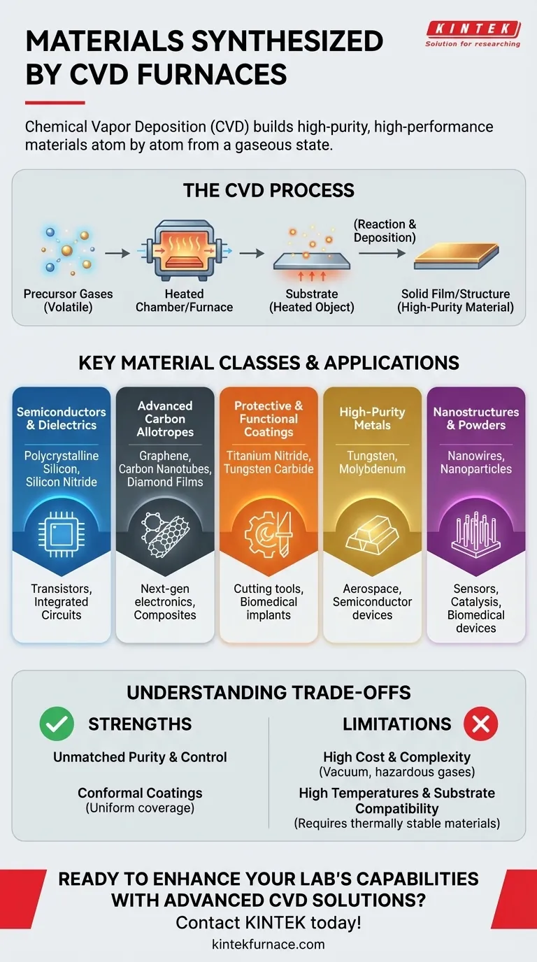
In short, a Chemical Vapor Deposition (CVD) furnace can synthesize an exceptionally broad range of materials. Its primary strength lies in creating high-purity, high-performance thin films and novel nanostructures. The most common material classes include advanced carbon allotropes like graphene and diamond, semiconductor films such as silicon, and durable protective coatings like carbides and nitrides.
Chemical Vapor Deposition is less about a specific list of materials and more about a fundamental principle: building solid materials, atom by atom, from a gaseous state. Its versatility makes it a foundational tool for creating materials with precisely controlled purity, structure, and performance.
The Principle: Building High-Performance Materials from Gas
How CVD Works
At its core, Chemical Vapor Deposition involves introducing one or more volatile precursor gases into a reaction chamber containing a heated object, known as a substrate.
The intense heat inside the furnace causes the gases to react or decompose on the substrate's surface. This chemical reaction results in the deposition of a solid, high-purity material directly onto the substrate, forming a thin film or coating.
Why This Method is Powerful
This gas-to-solid process allows for incredible control over the material's properties. By precisely managing temperature, pressure, and gas composition, engineers can dictate the thickness, crystal structure, purity, and morphology of the final product in a way that bulk manufacturing methods cannot.
A Breakdown of Key Material Classes
CVD's versatility allows it to produce materials for nearly every advanced engineering discipline. These can be grouped into several key categories.
Semiconductor and Dielectric Films
This is a cornerstone application of CVD. The process is used to deposit the ultra-pure crystalline layers that form the basis of modern electronics.
Key examples include polycrystalline silicon, silicon nitride, and various metal oxides used to build transistors, integrated circuits, and diodes.
Advanced Carbon Allotropes
CVD is a leading method for synthesizing some of the most advanced materials known. It can create highly ordered carbon structures with exceptional properties.
This category includes graphene (single-atom-thick sheets), carbon nanotubes, and synthetic diamond films, all used in next-generation electronics, composites, and coatings.
Protective and Functional Coatings
CVD excels at creating hard, dense, and resilient coatings that protect underlying components from wear, corrosion, and extreme temperatures.
Materials like titanium nitride, tungsten carbide, and other metallic carbides and nitrides are deposited on cutting tools, turbine blades, and biomedical implants to drastically extend their operational life.
High-Purity Metals
The process can also be used to deposit pure metallic films, including refractory metals that have very high melting points.
Examples include tungsten and molybdenum, which are used in high-temperature applications within the semiconductor and aerospace industries.
Nanostructures and Powders
By tuning the process parameters, CVD can be used to grow materials with specific nanoscale morphologies rather than just flat films.
This includes synthesizing nanowires, nanoparticles, and other structures with unique electrical and catalytic properties for use in sensors, catalysis, and biomedical devices.
Understanding the Trade-offs
While powerful, CVD is not the right choice for every application. Understanding its specific strengths and limitations is critical for making an informed decision.
Strength: Unmatched Purity and Control
The primary advantage of CVD is the ability to create materials with exceptional purity and structural perfection. Because the material is built from a filtered gas phase, contaminants are minimized. The process also creates conformal coatings, meaning it can uniformly coat complex, non-flat surfaces.
Limitation: Process Complexity and Cost
CVD systems require a vacuum environment, precise temperature control, and careful handling of precursor gases, some of which can be hazardous. This complexity makes the equipment and the process itself significantly more expensive than simpler methods like painting or electroplating.
Limitation: High Temperatures and Substrate Compatibility
CVD is fundamentally a high-temperature process. The substrate must be able to withstand the deposition temperature without melting, warping, or degrading. This limits the choice of substrate materials to those that are thermally stable, such as ceramics, graphite, tool steels, and high-temperature alloys.
Making the Right Choice for Your Goal
Deciding whether to use CVD depends entirely on your performance requirements.
- If your primary focus is advanced electronics: CVD is the industry standard for depositing the essential, ultra-pure semiconductor and dielectric films required for transistors and integrated circuits.
- If your primary focus is mechanical performance: CVD is the premier choice for applying hard, wear-resistant, and low-friction coatings to tools, engine parts, and medical implants.
- If your primary focus is materials research: CVD is an indispensable tool for synthesizing and exploring next-generation materials like graphene, carbon nanotubes, and novel nanomaterials.
Ultimately, CVD is the foundational technology for engineering materials with precisely tailored properties from the atomic level up.
Summary Table:
| Material Class | Key Examples | Common Applications |
|---|---|---|
| Semiconductor and Dielectric Films | Polycrystalline silicon, Silicon nitride | Transistors, Integrated circuits |
| Advanced Carbon Allotropes | Graphene, Carbon nanotubes, Diamond films | Next-gen electronics, Composites |
| Protective and Functional Coatings | Titanium nitride, Tungsten carbide | Cutting tools, Biomedical implants |
| High-Purity Metals | Tungsten, Molybdenum | Aerospace, Semiconductor devices |
| Nanostructures and Powders | Nanowires, Nanoparticles | Sensors, Catalysis, Biomedical devices |
Ready to enhance your lab's capabilities with advanced CVD furnace solutions? At KINTEK, we leverage exceptional R&D and in-house manufacturing to provide high-temperature furnace solutions tailored for diverse laboratories. Our product line includes Muffle, Tube, Rotary Furnaces, Vacuum & Atmosphere Furnaces, and CVD/PECVD Systems, complemented by strong deep customization to precisely meet your unique experimental requirements. Whether you're working on electronics, protective coatings, or nanomaterials research, we can help you achieve superior material synthesis. Contact us today to discuss how our solutions can drive your innovation forward!
Visual Guide
Related Products
- Custom Made Versatile CVD Tube Furnace Chemical Vapor Deposition CVD Equipment Machine
- Split Chamber CVD Tube Furnace with Vacuum Station CVD Machine
- Multi Heating Zones CVD Tube Furnace Machine for Chemical Vapor Deposition Equipment
- Slide PECVD Tube Furnace with Liquid Gasifier PECVD Machine
- Controlled Inert Nitrogen Hydrogen Atmosphere Furnace
People Also Ask
- What improvements can be made to the bonding force of gate dielectric films using a CVD tube furnace? Enhance Adhesion for Reliable Devices
- Which industries and research fields benefit from CVD tube furnace sintering systems for 2D materials? Unlock Next-Gen Tech Innovations
- What is a CVD tube furnace and what is its primary function? Discover Precision Thin-Film Deposition
- Why are CVD tube furnace sintering systems indispensable for 2D material research and production? Unlock Atomic-Scale Precision
- How can integrating CVD tube furnaces with other technologies benefit device fabrication? Unlock Advanced Hybrid Processes


