At its core, a Chemical Vapor Deposition (CVD) furnace is a highly versatile tool capable of depositing a vast range of materials. These materials are generally grouped into key categories, including semiconductors like silicon, pure metals and alloys like tungsten, and advanced ceramics such as carbides, nitrides, and oxides used for protective coatings and electronics.
The true value of CVD is not just the extensive list of materials it can deposit, but its precise control over the material's final form and properties. This allows for the engineering of films that are conductive, insulating, or exceptionally hard, tailored to a specific industrial or research need.
The Fundamental Building Blocks: Material Classes in CVD
CVD works by introducing precursor gases into a chamber, which then react and decompose on a substrate surface to form a solid film. The choice of precursor chemicals dictates the final material deposited.
Semiconductors and Elemental Materials
The most significant material deposited by CVD is silicon (Si), which forms the foundation of the entire semiconductor and microelectronics industry.
Beyond silicon, CVD is used to deposit other critical elements, most notably carbon. This can be in advanced forms like ultra-strong graphene or hard, low-friction diamond-like carbon (DLC) films.
Pure Metals and Metal Alloys
CVD is widely used to create thin films of pure metals. These are often chosen for their conductivity, resistance to heat, or barrier properties.
Common examples include tungsten (W), tantalum (Ta), and rhenium (Re). These metallic layers are essential in fabricating the complex, multi-layered structures inside integrated circuits.
Advanced Ceramics (Carbides and Nitrides)
This class of materials is renowned for extreme hardness, high-temperature stability, and chemical inertness, making them ideal for protective coatings.
Notable CVD ceramics include titanium nitride (TiN), which provides a hard, gold-colored coating on cutting tools, and robust structural materials like silicon carbide (SiC) and tungsten carbide (WC).
Dielectric and Oxide Ceramics
In contrast to conductive metals, CVD can also deposit electrically insulating (dielectric) materials. These are fundamental components in electronics.
Silicon dioxide (SiO2) is a primary insulator used in transistors. Other specialized oxides like alumina (Al2O3), zirconia (ZrO2), and hafnia (HfO2) are deposited for applications requiring specific dielectric properties or thermal stability.
Beyond Material Type: Controlling Structure
The versatility of CVD extends beyond the chemical composition to the physical structure of the deposited film. This control is critical for tuning a material's performance.
Polycrystalline and Amorphous Films
CVD can produce polycrystalline films, which consist of many small crystalline grains. These materials, such as polycrystalline silicon, are a cornerstone of solar panel and electronic device manufacturing.
Alternatively, the process can be adjusted to create amorphous films, which lack an ordered crystalline structure. Amorphous silicon, for instance, is vital for flexible electronics and some optical applications.
Complex and Novel Structures
Modern CVD techniques are not limited to simple, flat films. The process is precise enough to synthesize complex, high-aspect-ratio structures.
This includes the growth of one-dimensional materials like nanowires and nanotubes, which are at the forefront of materials science research for next-generation electronics and composites.
Understanding the Trade-offs of CVD
While incredibly powerful, the CVD process has inherent complexities and limitations that must be considered.
The Challenge of Precursor Chemicals
The CVD process is entirely dependent on its precursor gases. These chemicals must be volatile enough to be transported in gas form but stable enough to not decompose prematurely. They can often be expensive, toxic, or highly flammable, requiring significant safety infrastructure.
Process Complexity and Control
Achieving a high-quality, uniform film requires precise and stable control over multiple parameters simultaneously. Factors like temperature, pressure, gas flow rates, and chamber chemistry must be meticulously managed, making the equipment and process development inherently complex.
Matching the Material to Your Application
Your choice to use CVD will depend on the specific material properties your project demands.
- If your primary focus is semiconductor manufacturing: CVD is the non-negotiable industry standard for depositing the foundational silicon, silicon dioxide, and tungsten layers in integrated circuits.
- If your primary focus is protective coatings: Look to CVD for creating extremely hard, wear-resistant, and heat-resistant ceramic films like silicon carbide (SiC) and titanium nitride (TiN).
- If your primary focus is advanced materials research: The unparalleled flexibility of CVD enables the synthesis of cutting-edge materials, including graphene, custom oxide ceramics, and nanostructures.
Ultimately, the power of CVD lies in its ability to transform carefully chosen gases into high-performance solid materials, making it a cornerstone technology for modern engineering.
Summary Table:
| Material Category | Examples | Key Applications |
|---|---|---|
| Semiconductors | Silicon (Si), Graphene, Diamond-like Carbon (DLC) | Microelectronics, Flexible Electronics |
| Metals | Tungsten (W), Tantalum (Ta), Rhenium (Re) | Integrated Circuits, Heat Resistance |
| Ceramics | Titanium Nitride (TiN), Silicon Carbide (SiC), Silicon Dioxide (SiO2) | Protective Coatings, Insulation |
Unlock the full potential of CVD for your laboratory! KINTEK specializes in advanced high-temperature furnace solutions, including CVD/PECVD Systems, Muffle, Tube, Rotary, Vacuum & Atmosphere Furnaces. With exceptional R&D and in-house manufacturing, we offer deep customization to precisely meet your unique experimental needs—whether for semiconductor production, protective coatings, or cutting-edge materials research. Contact us today to discuss how our tailored solutions can enhance your efficiency and results!
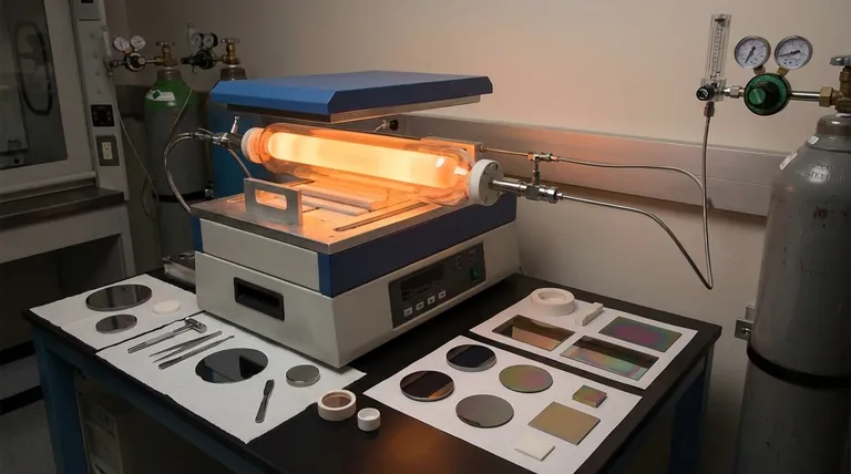
Visual Guide

Related Products
- Custom Made Versatile CVD Tube Furnace Chemical Vapor Deposition CVD Equipment Machine
- Split Chamber CVD Tube Furnace with Vacuum Station CVD Machine
- Multi Heating Zones CVD Tube Furnace Machine for Chemical Vapor Deposition Equipment
- Slide PECVD Tube Furnace with Liquid Gasifier PECVD Machine
- Controlled Inert Nitrogen Hydrogen Atmosphere Furnace
People Also Ask
- What customization options are available for CVD tube furnaces? Tailor Your System for Superior Material Synthesis
- What are the key application fields of CVD tube furnaces? Unlock Precision in Thin-Film Synthesis
- What future trends are expected in the development of CVD tube furnaces? Discover Smarter, More Versatile Systems
- What are the benefits of developing new precursor materials for CVD tube furnaces? Unlock Advanced Thin-Film Synthesis
- What temperature range do standard CVD tube furnaces operate at? Unlock Precision for Your Material Deposition


