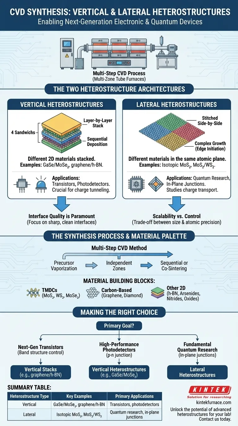
Specifically, these CVD systems are proven for synthesizing both vertical and lateral heterostructures. Key examples successfully created include vertically stacked materials like GaSe/MoSe₂, laterally stitched isotopic MoS₂, and other well-known combinations such as graphene/h-BN and MoS₂/WS₂. This is typically achieved using a controlled, multi-step CVD process.
The core capability of these systems is not just the growth of a single material, but the precise, layer-by-layer assembly of different two-dimensional (2D) materials. This control over heterostructure architecture is what enables the development of next-generation electronic and quantum devices.
The Two Architectures of Heterostructures
To understand what can be synthesized, you must first understand the two fundamental configurations of heterostructures that CVD can produce. These architectures define the material's properties and potential applications.
Vertical Heterostructures
A vertical heterostructure is created by stacking different 2D materials on top of one another, much like a sandwich. Each layer is a distinct material.
This is achieved through a sequential deposition process where one material is grown first, followed by the introduction of new precursors to grow the second material directly on its surface.
Examples like GaSe/MoSe₂ and graphene/h-BN fall into this category. This architecture is essential for creating devices where charge needs to tunnel or transfer between layers, such as in transistors and photodetectors.
Lateral Heterostructures
A lateral heterostructure consists of different materials stitched together side-by-side within the same atomic plane. Instead of a stack, you create a single, continuous 2D sheet with distinct domains.
This is a more complex process where growth conditions are carefully managed to initiate the growth of a second material at the edges of the first.
The synthesis of isotopic MoS₂ is a prime example, where molybdenum sulfide is grown using different isotopes of sulfur, creating a perfect crystal lattice with distinct isotopic domains. This is crucial for studying in-plane electronic junctions and quantum phenomena without the complexity of a vertical interface.
The Synthesis Process and Material Palette
The versatility of these systems comes from the CVD process itself, which allows for a wide range of material "building blocks."
The Multi-Step CVD Method
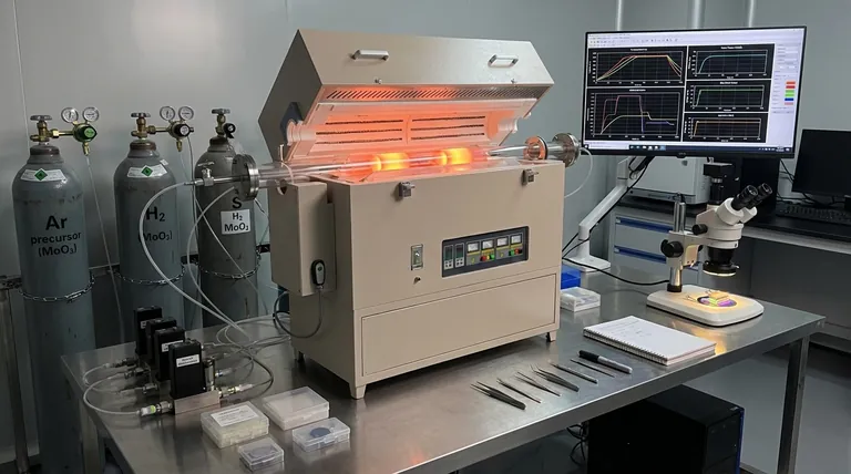
The successful synthesis of heterostructures relies on a two-step or multi-step CVD method. This is often performed in multi-zone tube furnaces.
These furnaces provide independent temperature zones, allowing for precise control over the vaporization and delivery of different precursor materials in sequence. This sequential or co-sintering process is the key to building complex structures.
Available Material Building Blocks
Heterostructures are built from the foundational 2D materials that CVD can produce. Beyond the specific examples mentioned, the process is suitable for a wide range of materials, including:
- Transition Metal Dichalcogenides (TMDCs): Such as MoS₂, WS₂, MoSe₂, etc.
- Carbon-Based Materials: Graphene and diamond films.
- Other 2D Materials: Hexagonal boron nitride (h-BN), arsenides, nitrides, and oxides.
Understanding the Trade-offs
While powerful, this synthesis method requires navigating critical technical challenges to achieve high-quality results.
Interface Quality is Paramount
The interface between the two different materials in a heterostructure is where the most interesting physics occurs, but it is also the most difficult part to control.
Lattice mismatch between materials can introduce strain, defects, and impurities, which can degrade device performance. Achieving a clean, sharp interface is a primary focus of process optimization.
Scalability vs. Control
There is often a trade-off between the size of the synthesized heterostructure and the precision of its atomic arrangement.
Growing small, pristine single-crystal heterostructures for research is well-established. However, scaling this up to wafer-scale production with uniform quality remains a significant engineering challenge for commercial applications.
Making the Right Choice for Your Goal
The type of heterostructure you aim to synthesize should be directly guided by your end application.
- If your primary focus is next-generation transistors: Pursue vertical stacks like graphene/h-BN or other TMDC combinations to control electronic band structure and tunneling properties.
- If your primary focus is high-performance photodetectors: Explore vertical heterostructures that form a p-n junction, such as GaSe/MoSe₂, to maximize light absorption and electron-hole separation.
- If your primary focus is fundamental quantum research: Consider lateral heterostructures to create pristine, in-plane junctions for studying charge transport and quantum confinement.
Mastering the controlled synthesis of these heterostructures is the gateway to designing materials with functionalities that do not exist in nature.
Summary Table:
| Heterostructure Type | Key Examples | Primary Applications |
|---|---|---|
| Vertical Heterostructures | GaSe/MoSe₂, graphene/h-BN | Transistors, photodetectors |
| Lateral Heterostructures | Isotopic MoS₂, MoS₂/WS₂ | Quantum research, in-plane junctions |
Unlock the potential of advanced heterostructures for your lab! KINTEK specializes in high-temperature furnace solutions, including CVD/PECVD Systems, with deep customization to meet your unique experimental needs. Whether you're developing next-generation electronics or conducting quantum research, our expertise in R&D and in-house manufacturing ensures precise control for synthesizing vertical and lateral heterostructures. Contact us today to discuss how we can enhance your synthesis processes and accelerate your innovations!
Visual Guide
Related Products
- 915MHz MPCVD Diamond Machine Microwave Plasma Chemical Vapor Deposition System Reactor
- Cylindrical Resonator MPCVD Machine System for Lab Diamond Growth
- HFCVD Machine System Equipment for Drawing Die Nano Diamond Coating
- MPCVD Machine System Reactor Bell-jar Resonator for Lab and Diamond Growth
- RF PECVD System Radio Frequency Plasma Enhanced Chemical Vapor Deposition
People Also Ask
- What is the MPCVD method and why is it considered effective for diamond deposition? Superior Purity & High Growth Rates
- What are the essential components of an MPCVD reactor for diamond film deposition? Unlock High-Quality Diamond Growth
- What is the purpose of a microwave plasma chemical vapor deposition system? Grow High-Purity Diamonds and Advanced Materials
- What is the basic principle of operation for the microwave plasma chemical vapor deposition system? Unlock High-Purity Material Growth
- What are the main components of an MPCVD machine? Unlock the Secrets of Diamond Synthesis


