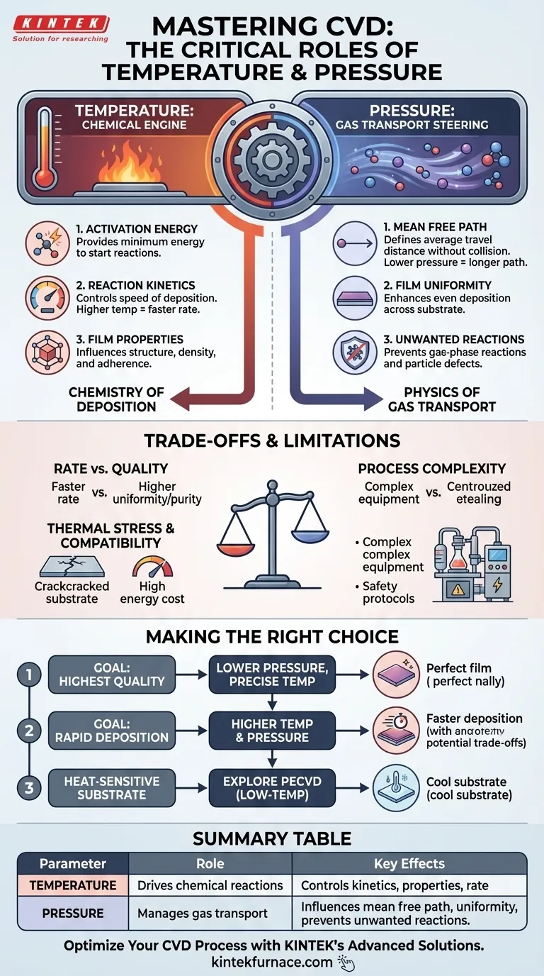
In Chemical Vapor Deposition (CVD), temperature and pressure are the two master controls governing the entire process. Temperature provides the fundamental energy required to drive the chemical reactions that create the film, while pressure dictates the physical environment, controlling how reactant gases travel and deposit onto the substrate. Getting this balance right is the key to successful deposition.
At its core, the relationship is simple: temperature governs the chemistry of the deposition, and pressure governs the physics of gas transport. Mastering CVD requires understanding how to manipulate this interplay to achieve your desired outcome, whether it's film quality, deposition speed, or cost-effectiveness.
The Role of Temperature: Driving the Chemical Reaction
Temperature is the engine of the CVD process. Without sufficient thermal energy, the precursor gases will not react, and no film will be deposited.
Providing Activation Energy
Every chemical reaction requires a minimum amount of energy to get started, known as activation energy. In CVD, the heated chamber provides this energy, causing precursor gases to either break down (decompose) or react with one another.
This is the fundamental step that transforms volatile gases into the solid material that forms the coating.
Dictating Reaction Kinetics
The specific temperature directly controls the reaction kinetics, or the speed at which the deposition reaction occurs. Higher temperatures generally lead to faster reaction rates and, consequently, a quicker build-up of the film.
Precise temperature control is therefore essential for achieving a predictable and repeatable deposition rate.
Influencing Final Film Properties
Temperature doesn't just affect speed; it profoundly influences the material properties of the final film. This includes its crystalline structure, density, and adherence to the substrate.
Incorrect temperature can result in poor film quality, internal stresses, or even the deposition of an entirely different material than intended.
The Role of Pressure: Controlling the Deposition Environment
If temperature is the engine, pressure is the steering. It manages the behavior of gas molecules within the reaction chamber, ensuring they arrive at the substrate surface in a controlled manner.
Defining the Mean Free Path
Pressure directly influences the mean free path—the average distance a gas molecule can travel before colliding with another molecule.
Lower pressures, often approaching a vacuum, increase the mean free path. This means reactant molecules are more likely to travel directly to the substrate surface without colliding with other molecules in the gas phase.
Enhancing Film Uniformity
A longer mean free path is critical for achieving a uniform film. When molecules travel unimpeded, they can deposit evenly across the entire surface of the substrate.
At higher pressures, more collisions occur in the gas phase, which can lead to reactants clumping together or depositing unevenly, degrading film quality.
Preventing Unwanted Gas-Phase Reactions
By reducing the frequency of molecular collisions, lower pressure helps prevent undesirable reactions from occurring in the gas phase above the substrate.
These gas-phase reactions can create particles that "rain down" onto the surface, creating defects and impurities in the film. Controlling pressure minimizes this effect, leading to a purer, higher-quality coating.
Understanding the Trade-offs and Limitations
Optimizing temperature and pressure is not a simple task of turning dials; it is a careful balancing act fraught with critical trade-offs.
The Central Conflict: Rate vs. Quality
The most common trade-off in CVD is between deposition rate and film quality. While higher temperatures and pressures can increase the deposition rate, they often do so at the expense of uniformity and purity.
Conversely, the conditions that produce the highest quality films—lower pressure and meticulously controlled temperatures—often result in slower, and therefore more expensive, deposition processes.
Substrate Compatibility and Thermal Stress
The high temperatures required for many CVD processes (often above 1000°C) severely limit the types of materials that can be used as substrates. Many polymers, and even some metals, cannot withstand such heat.
Furthermore, these high temperatures are a significant source of equipment wear and high energy costs, adding to the overall expense of the process.
Process Complexity and Safety
CVD is an inherently complex process. It demands sophisticated equipment for precise temperature and pressure control and involves the use of precursor gases that are often hazardous, toxic, or flammable.
This complexity increases both the initial equipment investment and the ongoing operational costs associated with safety protocols and maintenance.
Making the Right Choice for Your Goal
Your optimal CVD parameters are defined by your primary objective. Use these principles as your guide.
- If your primary focus is the highest film quality and uniformity: Prioritize lower pressures to maximize the mean free path and use precise, stable temperature control to ensure consistent reaction kinetics.
- If your primary focus is a rapid deposition rate: You may need to operate at higher temperatures and pressures, but be prepared to analyze and accept a potential reduction in film uniformity and purity.
- If your primary focus is compatibility with a heat-sensitive substrate: Standard high-temperature CVD is likely unsuitable; you must explore low-temperature alternatives like Plasma-Enhanced CVD (PECVD).
Ultimately, mastering the roles of temperature and pressure transforms CVD from a complex procedure into a powerful and precise manufacturing tool.
Summary Table:
| Parameter | Role in CVD | Key Effects |
|---|---|---|
| Temperature | Drives chemical reactions | Controls reaction kinetics, film properties, and deposition rate |
| Pressure | Manages gas transport | Influences mean free path, uniformity, and prevents gas-phase reactions |
Optimize Your CVD Process with KINTEK's Advanced Solutions
Struggling to balance temperature and pressure for superior film quality or faster deposition rates? At KINTEK, we leverage exceptional R&D and in-house manufacturing to provide diverse laboratories with advanced high-temperature furnace solutions. Our product line, including Muffle, Tube, Rotary Furnaces, Vacuum & Atmosphere Furnaces, and CVD/PECVD Systems, is complemented by strong deep customization capabilities to precisely meet your unique experimental requirements. Whether you need enhanced film uniformity, rapid deposition, or compatibility with heat-sensitive substrates, our tailored solutions deliver reliable performance and cost-effectiveness.
Contact us today via our contact form to discuss how we can help you master CVD for your specific goals!
Visual Guide
Related Products
- Custom Made Versatile CVD Tube Furnace Chemical Vapor Deposition CVD Equipment Machine
- Split Chamber CVD Tube Furnace with Vacuum Station CVD Machine
- Multi Heating Zones CVD Tube Furnace Machine for Chemical Vapor Deposition Equipment
- Slide PECVD Tube Furnace with Liquid Gasifier PECVD Machine
- Controlled Inert Nitrogen Hydrogen Atmosphere Furnace
People Also Ask
- How does CVD tube furnace sintering enhance graphene growth? Achieve Superior Crystallinity and High Electron Mobility
- What are the key application fields of CVD tube furnaces? Unlock Precision in Thin-Film Synthesis
- What are the practical applications of gate media prepared by CVD tube furnaces? Unlock Advanced Electronics and More
- What are the benefits of developing new precursor materials for CVD tube furnaces? Unlock Advanced Thin-Film Synthesis
- Which industries and research fields benefit from CVD tube furnace sintering systems for 2D materials? Unlock Next-Gen Tech Innovations


