At its core, a Chemical Vapor Deposition (CVD) furnace is a foundational tool in the semiconductor industry, responsible for building the microscopic layers that form an integrated circuit. These furnaces use a controlled chemical reaction to deposit exceptionally thin, pure, and uniform films of material onto silicon wafers. This process is the primary method for creating the insulating, conductive, and semiconducting layers that are the building blocks of transistors and all other modern electronic components.
The essential role of a CVD furnace is not merely to deposit material. Its true value lies in the unmatched precision it provides, allowing engineers to control film thickness, composition, and uniformity at the atomic level—a non-negotiable requirement for manufacturing reliable, high-performance microchips.
The Fundamental Process: From Gas to Solid
To understand the role of a CVD furnace, you must first understand the process it facilitates. It is fundamentally a method for building solid materials from the bottom up.
The Core Principle: A Controlled Chemical Reaction
CVD introduces specific precursor gases into a high-temperature, vacuum-controlled chamber containing silicon wafers. The heat provides the energy for these gases to react and decompose on the wafer's surface. As they react, they form a new, stable, solid thin film that is chemically bonded to the surface below it.
The Furnace as the Reaction Environment
The furnace itself is the critical piece of equipment that enables this process with extreme precision. It meticulously controls the key variables: temperature, pressure, and the flow of precursor gases. This control ensures the resulting film has the exact properties required, from its thickness to its chemical makeup.
Critical Roles in Chip Fabrication
CVD is not a single-use process; it is a versatile technique used repeatedly during the manufacturing of a single chip to build its complex, three-dimensional structure.
Depositing Insulating Layers (Dielectrics)
Modern microchips contain billions of transistors packed into a tiny space. To prevent electrical signals from interfering with each other, these components must be electrically isolated. CVD is used to deposit high-quality insulating films, such as silicon dioxide (SiO₂) and silicon nitride (Si₃N₄), which act as barriers between conductive pathways.
Forming Semiconducting and Conductive Films
The "gate" of a transistor, which controls its on/off state, is often made from a material called polysilicon. CVD is the primary method for depositing this critical semiconducting film. This polysilicon layer can also be modified (doped) to become conductive, forming part of the chip's intricate wiring.
Enabling Perfect Crystal Growth (Epitaxy)
For certain high-performance devices, a flawless crystal layer must be grown on top of the base silicon wafer. This process, known as epitaxial growth, is a specialized form of CVD that creates a perfect, defect-free foundation for building superior transistors.
Understanding the Trade-offs and Challenges
While indispensable, the CVD process is not without significant engineering challenges. Success in semiconductor manufacturing depends on mastering these complexities.
The Unyielding Demand for Purity
The chemical reactions in CVD are extremely sensitive to contamination. Even a few stray atoms of an unwanted element can introduce a defect that ruins an entire microchip. This requires ultra-pure precursor gases and immaculately clean furnace chambers, driving up operational complexity and cost.
The Pursuit of Absolute Uniformity
For a chip to function correctly, every transistor must behave identically. This means the deposited films must have the exact same thickness and composition across the entire surface of a 300mm wafer. Achieving this level of uniformity is a constant focus of process engineers.
High Cost and Complexity
CVD furnaces are highly sophisticated and expensive pieces of capital equipment. They require significant expertise to operate, maintain, and calibrate. The development of new CVD processes for next-generation chips is a major area of research and development in the industry.
Making the Right Choice for Your Goal
The application of CVD principles is vast, but your focus will shift depending on your specific objective.
- If your primary focus is integrated circuit design: You must understand that the physical properties of CVD films define the performance limits and reliability of the transistors and interconnects you are designing.
- If your primary focus is process engineering: Your goal is to optimize CVD "recipes"—the specific combination of temperature, pressure, and gas flow—to maximize film uniformity, purity, and throughput, which directly impacts manufacturing yield and cost.
- If your primary focus is materials science: CVD is a fundamental tool for synthesizing an enormous range of thin films and novel materials, from the semiconductors in a phone to the superhard coatings on a turbine blade.
Ultimately, Chemical Vapor Deposition is the cornerstone technology that transforms simple gases into the complex, functional heart of all modern electronics.
Summary Table:
| Application | Key Function | Materials Deposited |
|---|---|---|
| Insulating Layers | Prevents electrical interference | Silicon Dioxide (SiO₂), Silicon Nitride (Si₃N₄) |
| Semiconducting/Conductive Films | Forms transistor gates and wiring | Polysilicon |
| Epitaxial Growth | Creates flawless crystal foundations | High-purity silicon layers |
Enhance your semiconductor or materials research with KINTEK's advanced CVD solutions! Leveraging exceptional R&D and in-house manufacturing, we provide high-temperature furnaces like CVD/PECVD Systems, Muffle, Tube, Rotary, Vacuum & Atmosphere Furnaces, tailored to your unique needs. Our deep customization ensures precise control for superior film uniformity and purity. Ready to optimize your processes? Contact us today to discuss how we can support your goals!
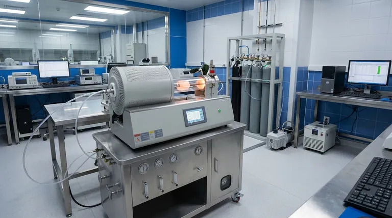
Visual Guide

Related Products
- Custom Made Versatile CVD Tube Furnace Chemical Vapor Deposition CVD Equipment Machine
- Split Chamber CVD Tube Furnace with Vacuum Station CVD Machine
- Multi Heating Zones CVD Tube Furnace Machine for Chemical Vapor Deposition Equipment
- Slide PECVD Tube Furnace with Liquid Gasifier PECVD Machine
- Controlled Inert Nitrogen Hydrogen Atmosphere Furnace
People Also Ask
- What future trends are expected in the development of CVD tube furnaces? Discover Smarter, More Versatile Systems
- What are the key application fields of CVD tube furnaces? Unlock Precision in Thin-Film Synthesis
- What is the working principle of a CVD tube furnace? Achieve Precise Thin Film Deposition for Your Lab
- Why are CVD tube furnace sintering systems indispensable for 2D material research and production? Unlock Atomic-Scale Precision
- Which industries and research fields benefit from CVD tube furnace sintering systems for 2D materials? Unlock Next-Gen Tech Innovations


